Continue to Site

Welcome to EDAboard.com

Welcome to our site! EDAboard.com is an international Electronics Discussion Forum focused on EDA software, circuits, schematics, books, theory, papers, asic, pld, 8051, DSP, Network, RF, Analog Design, PCB, Service Manuals... and a whole lot more! To participate you need to register. Registration is free. Click here to register now.

Chopper Amplifier Design

Status
Not open for further replies.

GiGa212

Newbie
Joined
Jul 15, 2022
Messages
3
Helped
0
Reputation
0
Reaction score
0
Trophy points
1
Activity points
68
Hi all!

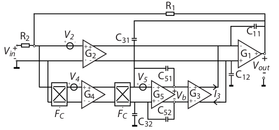
I'm a Jr. Analog IC Designer that are trying to design, for the first time, a chopper amplifier based on the following structure:
chopper.png


I've already designed all blocks, and now I'm simulating the entire system (transient, pss, etc.) in buffer mode, with a DC input equal to VDD/2, and chopper freq equal to 16kHz (that freq. is greater than the 1/f corner of the core stage G2+G1).
During transient simulation I noticed a strange behavior (I think) of the output; in practice I expect that the output should be synchronous with the chopping frequency, but in reality the behavior is the following:
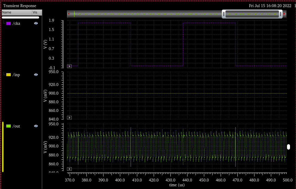
tran.png


My question is:
is it correct that the output oscillates faster than the chopping freq.? If yes, do you know what is the problem?


Thanks.
 

is it correct that the output oscillates faster than the chopping freq.? If yes, do you know what is the problem?
No, I believe you are seeing an oscillation.

If so, you need to look at the Bode plot of the amplifier open loop response and see if the gain/phase margin is adequate.
Does the amp have a dominate 1-pole rolloff from near DC to the 0dB gain point?
 

Hi crutschow, and thanks for your reply.

The core OA made by G2+G1 is a rail-to-rail class-AB OA having PM of 68.5°; G4 is a fd-folded cascode with cmfb having PM of 99 and Loop PM 86°; G5 is a one stage diff. amp. with cmfb having PM of 117.3° and Loop PM of 84°. So, I think that all blocks are stable.

The Bode plot of the entire system is the following:
bode.png


Its behavior near 0dB its strange, but the function phasemargin of Cadence calculator gives a PM of 66.54.
 

Hi,

You have multiple loops and compensation points. Not just sub-block stability parameters are interesting, the sub-blocks connected together also form new loops. Furthermore, CMFB was not highlighted on your 1st figure, which must be stable too.

So,
a, did you check CMFB stability parameters too?
b, did you check all DMFB loops stability separately after connecting the sub-blocks?

btw, the system bode plot doesn't look stable, don't believe for calculator. Because of class-AB structures I guess, the phase goes up 1st, but that not so important, the point is that the phase changes more than 180deg before loop gain magnitude drops to unity
(+90deg at 1mHz, -120deg at 100MHz, 0dB freq ~100MHz -> 90+120=210deg before 0dB freq).

You have too much gain in the system and the dominant pole freq is too high. Decrease consumption of the transconductance responsible for the dominant pole (G2 maybe?), it will increase its output resistance, so its pole freq, and decrease its gm, so its gain contribution, or increase compensation capacitance value (C11 maybe?). I think these can be a solution for your issue, not sure.
 

It is definitely not stable. I visually counted the oscillation periods within one chop period and without claiming any degree of accuracy I think that the oscillation frequency is close to where the loop crosses 0dB or where the phase starts dropping sharply.
 

Hi all!
Thanks for your replies.

I'm pretty sure that all blocks are stable if taken singularly, but the problem rise when all blocks are connected together. In the last two days I tried to find a way to compensate the overall system based on the analysis @frankrose , but without success.
Capacitors C31/C32 acts only to compensate the -40dB/dec roll-off by adding a low frequency zero, so don't do anything in the high frequency range.
On the other hand, in my situation, capacitors C11/C12 are the compensating capacitances connected as cascode Miller of the core OA i.e., G1/G2 which is a I/O rail-to-rail calss-AB, and its Bode plot is the following
1658390374449.png

I think that the problem of the sharp drop of the phase of the entire system is due to G1/G2, bu t I'm not sure.

@sutapanaki Yes, you're right! The oscillation frequency of the output is approximately 1MHz i.e., when the phase starts to drop.
 

Why don't you start simple? Check the stability of your main amplifier G1+G2 first, but have the loading at the input of G1 coming from the chopping circuitry. For example, you can disconnect the first chopper from the input of G2 and connect the inputs of the chopper to gnd, since they are at virtual ground anyway. Disable chopping by setting one side of the chopping switches on and the other off. Make sure the outputs of G3 don't rail, so that you can have proper loading there. And then run maybe first DC to check the operating point and then stb for the stability.
 

Status
Not open for further replies.

Part and Inventory Search

Welcome to EDABoard.com

Sponsor

Back
Top