Continue to Site

Welcome to EDAboard.com

Welcome to our site! EDAboard.com is an international Electronics Discussion Forum focused on EDA software, circuits, schematics, books, theory, papers, asic, pld, 8051, DSP, Network, RF, Analog Design, PCB, Service Manuals... and a whole lot more! To participate you need to register. Registration is free. Click here to register now.

Charge pump topology

Status
Not open for further replies.

bharath_k

Junior Member level 3
Joined
Jun 8, 2018
Messages
31
Helped
0
Reputation
0
Reaction score
0
Trophy points
6
Activity points
244
Hi everyone,

I have a task to design a charge pump to generated a output voltage of 3.3 V from 0.8 V supply with load current of 8 mA in 22nm technology. I started off with a Dickson charge pump and also tried pelliconi charge pump. But in both cases the output current is in micro amperes range. I am using 1Mhz clock and 10pf Cfly. Can anyone please suggest me a better topology to maximize my output current and any design methods which I should follow.

Thanks!
 

charge pump
...
0.8 V supply

It's a challenge since you want to build an oscillating circuit which avoids the use of diodes because they subtract from output voltage.

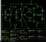
This simulation is a voltage doubler which works with transistors, and 0.8V supply. It illustrates what's possible if it could be adapted to your spec 22nm.

astable H-bridge 6 transis 1V supply 2 cap V dblr 300 ohm load gets 1_8V.png

The stacked capacitors receive alternating current at the center of an H-bridge (consisting of the two rightmost half-bridges). Each capacitor acquires supply voltage.

Clock signals originate in the left H-bridge (consisting of the two leftmost half-bridges).
Thus the middle half-bridge does double duty.

- - - Updated - - -

Conceivably you could install an identical voltage doubler where the load is, thus making a self-oscillating voltage quadrupler, from a 0.8V supply.
 

Hi Brad,

Thanks for your reply. May be I didn't explain my application clear. I don't want an oscillating circuit. I want a DC-DC converter. The application where this charge pump to be used is for Neurostimulation.

Thanks.
 

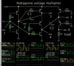
This voltage multiplier is a Nakagome type. Capacitors charge in parallel, discharge in series.

Additional stages can be added until output is 3.3 V to your load. This schematic is a tripler, to demonstrate how stages are cascaded. The method is to attach half-bridges in combination. It may be possible to get correct bias for each transistor by tapping for voltage changes at strategic nodes.

Nakagome tripler clk-driven 500kHz 2 caps 7 transis 0_8V supply.png

Clock pulses are applied at left (which you shall provide since you claim you don't need an oscillator).
 
Thanks a lot. I will work on this and let you know the result.
 

Status
Not open for further replies.

Part and Inventory Search

Welcome to EDABoard.com

Sponsor

Back
Top