Juja
Newbie level 3
Hi there!
I want to use the KAF1001-CCD for image processing (https://www.onsemi.com/pub_link/Collateral/KAF-1001-D.PDF).
I have some understanding problems with the clocking/timing of V1 and V2 according to set the integration time.
In the datasheet on Page4 it is written:
"Referring to the timing diagram, integration of charge is performed with fV1 and fV2 held low."
So for me the integration time is just the "low time" of V1/V2.
What I don't get then is the Frame Timing Diagram (Page12):
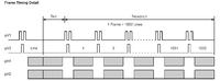
For me it looks like that the integration time is set "in front" of the read out of every frame.
But when the sentence on Page4 is correct, the integration time is set between every single line (V1/V2 is set low between every single line)
Can somebody help me with the understanding in how to set the integration time exactly?!
Thnaks so far!
Juja
I want to use the KAF1001-CCD for image processing (https://www.onsemi.com/pub_link/Collateral/KAF-1001-D.PDF).
I have some understanding problems with the clocking/timing of V1 and V2 according to set the integration time.
In the datasheet on Page4 it is written:
"Referring to the timing diagram, integration of charge is performed with fV1 and fV2 held low."
So for me the integration time is just the "low time" of V1/V2.
What I don't get then is the Frame Timing Diagram (Page12):
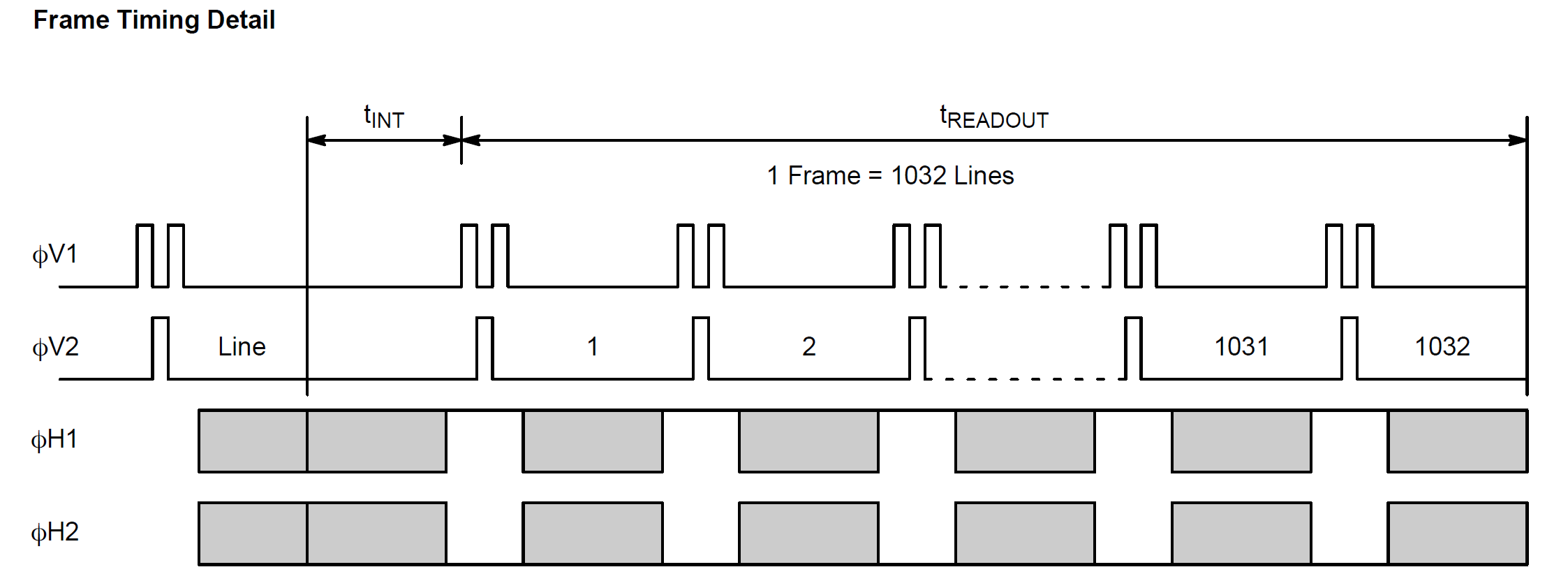
For me it looks like that the integration time is set "in front" of the read out of every frame.
But when the sentence on Page4 is correct, the integration time is set between every single line (V1/V2 is set low between every single line)
Can somebody help me with the understanding in how to set the integration time exactly?!
Thnaks so far!
Juja