Continue to Site

Welcome to EDAboard.com

Welcome to our site! EDAboard.com is an international Electronics Discussion Forum focused on EDA software, circuits, schematics, books, theory, papers, asic, pld, 8051, DSP, Network, RF, Analog Design, PCB, Service Manuals... and a whole lot more! To participate you need to register. Registration is free. Click here to register now.

Cascode current mirror circuit design

Status
Not open for further replies.

Rohbinhoodie

Newbie level 5
Joined
May 2, 2022
Messages
8
Helped
0
Reputation
0
Reaction score
0
Trophy points
1
Activity points
82
I want to make this circuit having more than 30dB voltage gain by controlling Length and width of the mosfets and biasing Vgs.
But literally I have no idea how to start with this.
Can you guys pls give me some useful tips?

+the mosfet is TSMC 180nm level 49.
+Vdd is 2.5v
+1.8um < L < 5um
+ 1.8um < w < 100um

Thank you for reading.
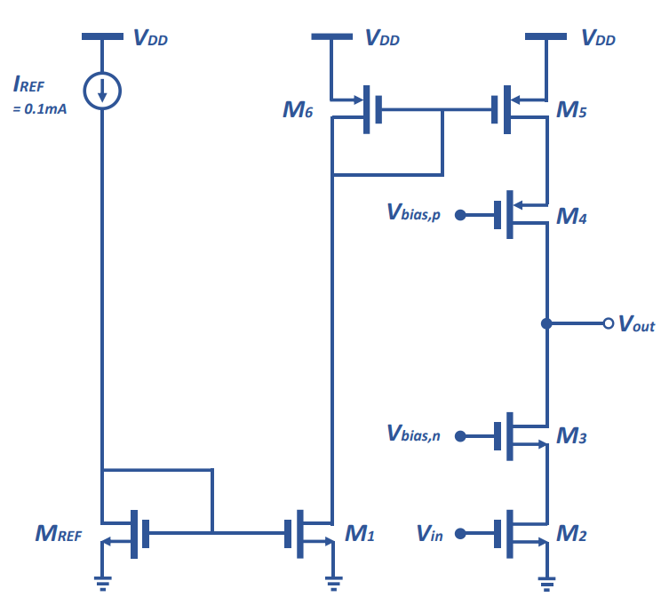
rrrtttt.PNG
 
Last edited:

Solution
30 dB shouldnt be an issue with that process.

If you do no thave any major constraints on output voltage swing at the moment, I would start by using a wideswing current mirror to bias the M3 and M4. Simply add a second "layer" on the two mirrors.

Set all L to be equal and for now set it as low as possible to start with. (Why do you have 1.8 um as minimum length? or is it a typo?)

Start by settings Widths of Mref, M1 and M2 equal, as well as M5 and M6 equal. M3 and new cascode transistor widhs equal, and M4 with its new cascodes equal as well.

That gives you 4 variables to play around with (W_{ref,1,2}, W_{5,6}, ..., etc.).

Start by making W_{ref,1,2} and W_{5,6} quite big to push down the voltages on those gates. Then align...
30 dB shouldnt be an issue with that process.

If you do no thave any major constraints on output voltage swing at the moment, I would start by using a wideswing current mirror to bias the M3 and M4. Simply add a second "layer" on the two mirrors.

Set all L to be equal and for now set it as low as possible to start with. (Why do you have 1.8 um as minimum length? or is it a typo?)

Start by settings Widths of Mref, M1 and M2 equal, as well as M5 and M6 equal. M3 and new cascode transistor widhs equal, and M4 with its new cascodes equal as well.

That gives you 4 variables to play around with (W_{ref,1,2}, W_{5,6}, ..., etc.).

Start by making W_{ref,1,2} and W_{5,6} quite big to push down the voltages on those gates. Then align the other widths.

Some googling gives you more tips on how to bias a current mirror and reduce the number of free variables.
 
Solution
30 dB shouldnt be an issue with that process.

If you do no thave any major constraints on output voltage swing at the moment, I would start by using a wideswing current mirror to bias the M3 and M4. Simply add a second "layer" on the two mirrors.

Set all L to be equal and for now set it as low as possible to start with. (Why do you have 1.8 um as minimum length? or is it a typo?)

Start by settings Widths of Mref, M1 and M2 equal, as well as M5 and M6 equal. M3 and new cascode transistor widhs equal, and M4 with its new cascodes equal as well.

That gives you 4 variables to play around with (W_{ref,1,2}, W_{5,6}, ..., etc.).

Start by making W_{ref,1,2} and W_{5,6} quite big to push down the voltages on those gates. Then align the other widths.

Some googling gives you more tips on how to bias a current mirror and reduce the number of free variables.
ahh sorry it was 0.18um.
is there any specific reason that I have to set widths of Mref, M1, M2 / M5, M6 equal?
 

is there any specific reason that I have to set widths of Mref, M1, M2 / M5, M6 equal?
You want to keep the symmetry in the design. Also, perhaps more importantly, you want to get down the number of free variables to be able to solve the problem.

Once you have a starting point, then you can look at ways to set for example the Wref smaller/larger to adjust currents, etc., in order to optimize, say power consumption.
Thank you for answering.
I have one more question.
Is it okay to have different width in cascode? I mean like for example, different width of NMOS M2 : L=0.18u W=50u // M3 : L=0.18u W=100u
 

" Is it okay to have different width in cascode? "

Yes, they are rarely the same width. However, quite often you use the same length for layout reasons.
 
" Is it okay to have different width in cascode? "

Yes, they are rarely the same width. However, quite often you use the same length for layout reasons.
Thank you so much.
sorry since I'm a student and I have no experience of designing circuit so I have a lot of questions.
Is there any tips setting the bias voltage, Vbiasp and Vbiasn?
 

Hello,

yes, the simplest approach is to set the bias voltages with the cascode current mirror topology. Use the voltages from the cascodes to drive your bias voltages.


Then there are refinements to be done, but easiest to do them iteratively. For example go to low-swing cascoded current mirror, etc, to save you one 2VT across the output, etc.


Status
Not open for further replies.

Part and Inventory Search

Welcome to EDABoard.com

Sponsor

Back
Top