Continue to Site

Welcome to EDAboard.com

Welcome to our site! EDAboard.com is an international Electronics Discussion Forum focused on EDA software, circuits, schematics, books, theory, papers, asic, pld, 8051, DSP, Network, RF, Analog Design, PCB, Service Manuals... and a whole lot more! To participate you need to register. Registration is free. Click here to register now.

can any one help me to find gain bandwidth product of the bode plot i attached

Status
Not open for further replies.
I think, following this philosophy, even the simplest opamp amplifier (inverting, non-inverting) would be classified as multiple feedback circuits.
I doubt, if this is a definition that makes sense. What about feedback caused by the collector-base capacitance of a BJT?
I prefer the usual view that treats the OP as black box with specified transfer characteristic and restricts the analysis to feedback in the external circuit.

Referring to the previous discussion it should be underlined, that a complex pole pair can be generated without multiple feedback pathes, as you can see from a second order Sallen Key filter with ideal amplifier.
 
  • Like
Reactions: LvW

    LvW

    Points: 2
    Helpful Answer Positive Rating
Assuming that the dominant pole in the OA is obtained with a feedback capacitor, then this is a sort of multiple feedback circuit (there are two nested loops), but not like the ones swown in posts #6 and #18.
I think, following this philosophy, even the simplest opamp amplifier (inverting, non-inverting) would be classified as multiple feedback circuits.
Yes. I just mean that the circut we are discussing about has multiple-feedback in that sense, not with the topology of posts #6 and #18.

What about feedback caused by the collector-base capacitance of a BJT?
As a matter of fact, this is the usual way the dominant pole is created in OA's since the 741, including the TL082.

I prefer the usual view that treats the OP as black box with specified transfer characteristic and restricts the analysis to feedback in the external circuit.
Me too, of course.

Referring to the previous discussion it should be underlined, that a complex pole pair can be generated without multiple feedback pathes, as you can see from a second order Sallen Key filter with ideal amplifier.

Right.
Regards
Z
 

As a matter of fact, this is the usual way the dominant pole is created in OA's since the 741, including the TL082.
I was, of course, referring to the internal C-B capacitance of a BJT (not to the compensation capacitor).
 

I was, of course, referring to the internal C-B capacitance of a BJT (not to the compensation capacitor).
Yes, of course I undertstood even if I didn't clarify the point.

If we want to go farther, let's say that an inverting lossy integrator (ideal OA with a parallel RC in feedback path) could be considered like an ideal integrator (with only C) with another "external" feedback loop formed by the R. An academic exercise, I think.
Regards

Z
 

If we want to go farther, let's say that an inverting lossy integrator (ideal OA with a parallel RC in feedback path) could be considered like an ideal integrator (with only C) with another "external" feedback loop formed by the R. An academic exercise, I think.
Regards
Z

Hi Zorro,
Did you check it by calculation? What is a "feedback loop formed by the R"? A loop consisting of one single resistor? I don`t think it works - even if considered as an academic exercise only. Do the calculation - and you will be convinced.
Regards
LvW
 

If you assume a gain block with an ideal first order low-pass transfer function (the said lossy integrator). Then external positive feedback can shift the pole towards zero (turn it into an ideal integrator). Or in other words, compensate the loss R with a negative resistor.

But in practice, the integrator won't be first order, and you'll have difficulties to compensate it excatly.
 

If you assume a gain block with an ideal first order low-pass transfer function (the said lossy integrator). Then external positive feedback can shift the pole towards zero (turn it into an ideal integrator). Or in other words, compensate the loss R with a negative resistor.
But in practice, the integrator won't be first order, and you'll have difficulties to compensate it excatly.

But - the above is not an answer to Zorro's last contribution, right?

- - - Updated - - -

More than that, I think this principle (1st order lowpass with positive feedback) is exploited in the non-inverting NIC integrator (Deboo integrator).
 

But - the above is not an answer to Zorro's last contribution, right?
I'm describing the condition under which you can compensate a lossy integrator. As far he's suggesting negative feedback (a resistor across an inverting OP circuit), I'm saying that it doesn't work.
 

no audioguru, i don't think that the response belongs to a second-order bandpass (why do you think of a mfb filter ?). Again: I think it's a circuit that differentiate (very poor phase margin as a typical property).
However, i think it's funny that we are guessing here - and the questioner (yadhu) does not tell us what kind of circuit he is investigating.

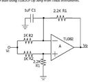
CIRCUIT.JPG this is the ckt i am analysing
 

Attachments

  • bodeplot.JPG
    bodeplot.JPG
    69.6 KB · Views: 53

Yes, yadhu - that was my first assumption: A (non-inverting) differentiator circuit.
Coming back to your original question - as mentioned in post#2 - you only can ask for the GBW of the opamp used, that means: not for the whole circuit.
The definition of the gain-bandwidth product needs a lowpass response.
 

then gbw for opamp is how much ? how to calculate it from the plot
 

then gbw for opamp is how much ? how to calculate it from the plot

As I have mentioned in post#2 already: The GBW is identical to the 0dB crossing of the open-loop gain function (approx. 2 MHz).
Note: This applies for all opamps exhibiting unity gain compensation (that means: first-order behaviour for open-loop gains > 0 dB).
In your case, this can be assumed.
 

Different from a simple N.I. differentiator, the present circuit has a voltage divider. At the 0 dB point of the transfer function, the OP has still a gain of 3.2 dB. Ends up in a GBW of 3 to 3.5 MHz, as expectable for TL082.
 
  • Like
Reactions: LvW

    LvW

    Points: 2
    Helpful Answer Positive Rating
Ohh yes, you are right of course! I forgot the factor introduced by the voltage divider. Thank you for correcting me.
 

Hi Zorro,
Did you check it by calculation? What is a "feedback loop formed by the R"? A loop consisting of one single resistor? I don`t think it works - even if considered as an academic exercise only. Do the calculation - and you will be convinced.
Regards
LvW
Hi,

I'm back in order to answer this point.

This is the circuit. I consider the output voltave vs. input current because in this way we have an input node and an output node (see 2nd figure below).
The total transfer function is the transimpedance V2/I1.

image001.gif

We can consider this circuit as a basic transfer function (in this case it is an ideal current-to-voltage integrator) with a feedback resitor, like this:

image002.gif

The topology of the feedback is node-node or voltage-current, i.e., a sample of the output voltage is taken at the output node and a current proportional to it is injected into the input node.
We will take the direct transfer funcion A and the feedback β, and then we will find the closed loop transfer funcion AF=A/(1+Aβ). The circuit for the transimpedance A, taking into account the load of the feedback part at both the input and the output is as follows:

image003.gif

In this particular case (ideal OA) R has no effect on either of the sides. The direct transfer function is A=V2/I1=-1/sC .
The feedback transfer function is the transconductance β=IF/V2|V1=0 in this two-port:

image004.gif

i.e. β=-1/R.

As said, the closed-loop transfer function is AF=A/(1+Aβ).
Replacing the obtained A and β, we get AF=-R/(1+sRC) .

Please let me know if it is clear or not.
Regards

Z
 

Please let me know if it is clear or not.

Hi Zorro - Yes, it’s clear, of course. Good exercise.

If we want to go farther, let's say that an inverting lossy integrator (ideal OA with a parallel RC in feedback path) could be considered like an ideal integrator (with only C) with another "external" feedback loop formed by the R. An academic exercise, I think.
Z

However, recalling the sentence as cited above (from your post #24) my remark in post#25 was related to an opamp-based circuit that is able to integrate voltages (classic MILLER integrator).
Your calculations show that the classic opamp-based circuit for current-to-voltage conversion (assumption: ideal opamp) with capacitive feedback has a transfer characteristic -1/sC and, thus, performs current integration (with sign inversion) - in principle, like each single grounded capacitor. Therefore, it is clear that another resistor in parallel will turn the circuit into a 1st-order current-in and voltage-out lowpass(damped integration). No doubt about it.

Regards
LvW
 

Yes, the inverting voltage integrator is what I've shown preceded by a two-port that performs voltage-to-current conversion (i.e. a resistor that "see" a very low load impedance, that in this case is the virtual ground).
An accurate analysis for a nonideal OA would take into account the input impedance of the second two-port, that is the impedance of the open-loop two-port divided by (1+Aβ).
Regards

Z
 
Last edited:

Status
Not open for further replies.

Part and Inventory Search

Welcome to EDABoard.com

Sponsor

Back
Top