ajeya
Newbie level 6
Hi,
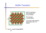
I am new to IC layout. I am finding it confusing to make a Power MOSFET (NMOS) width 9.2mm width and length 1.6u. As per schematic simulation study.
This seems to big to be drawn like simple nmos of small Width(um)and Length (um)
Can some one point me to the right resource or give suggestion on how to draw this Power MOSFET.
Thanks.
