Continue to Site

Welcome to EDAboard.com

Welcome to our site! EDAboard.com is an international Electronics Discussion Forum focused on EDA software, circuits, schematics, books, theory, papers, asic, pld, 8051, DSP, Network, RF, Analog Design, PCB, Service Manuals... and a whole lot more! To participate you need to register. Registration is free. Click here to register now.

Cadence Virtuoso errors in DRC layout

Status
Not open for further replies.

yyjjjj

Newbie
Joined
Nov 19, 2021
Messages
1
Helped
0
Reputation
0
Reaction score
0
Trophy points
1
Activity points
17
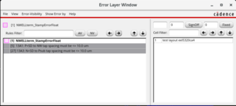
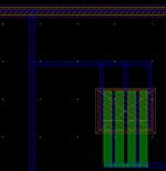
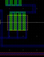
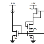
Hi, I'm a newbie for cadence virtuoso layout. When I ran the DRC report, I met three errors. I struggled a long time. Error 1 and 2 are the same MOSFET. It's PMOS. It's screenshot 6. Error 3 is screenshot 7. It's NMOS. I also attached the schematic. It's screenshot 9. May I know how to deal with those three errors? Appreciate it a lot.
 

Attachments

  • Screenshot_5.png
    Screenshot_5.png
    33 KB · Views: 143
  • Screenshot_6.png
    Screenshot_6.png
    87.5 KB · Views: 124
  • Screenshot_8.png
    Screenshot_8.png
    75.5 KB · Views: 124
  • Screenshot_9.png
    Screenshot_9.png
    6.8 KB · Views: 119

Check if you have put the substrate taps within 10um distance from the respective source/drain diffusion areas. That is the error you are facing.
 

Status
Not open for further replies.

Similar threads

Part and Inventory Search

Welcome to EDABoard.com

Sponsor

Back
Top