Continue to Site

Welcome to EDAboard.com

Welcome to our site! EDAboard.com is an international Electronics Discussion Forum focused on EDA software, circuits, schematics, books, theory, papers, asic, pld, 8051, DSP, Network, RF, Analog Design, PCB, Service Manuals... and a whole lot more! To participate you need to register. Registration is free. Click here to register now.

[SOLVED] Cadence Virtuoso - Design Rule Check clearing erros

Status
Not open for further replies.

lifeislife

Newbie level 4
Joined
Oct 16, 2022
Messages
6
Helped
0
Reputation
0
Reaction score
0
Trophy points
1
Activity points
41
Hello,


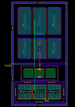
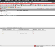
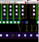
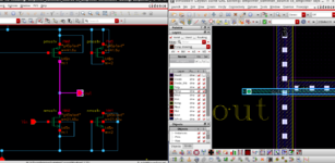
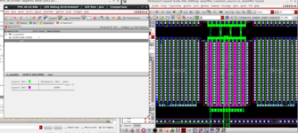
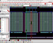
I am completely new to this, I am trying to complete a module on Cadence Virtuoso Education kit. However, I got stuck on clearing some errors related to Design Rule Check (DRC). The circuit built is attached and layout. Anyone can help on this are these errors or just warnings I can ignore and proceed, please advice.

Thank you.


Layout.png
Schematic.png


PVS_DRC Result Viewer.png
PVS_Reports DRC.png


PVS_Reports DRC_1.png
PVS_Reports DRC_2.png
 

You have created a latchup by violating the rule about maximum distance between contacts to well or substrate.
On your layout i can see two guard rings, one connected to gnd around nfets (if it is made on psub then is good) and one large connected to vdd - if this one is the only one for nwell then you have issue here. Remove this outer ring, enclose every pfet with such nwell ring.
 
Thank you for your reply. nWell around pfet was missing solved it errors cleared
--- Updated ---

However there is another error in LVS. Unmatched schematic pin labels. I tried tracing it back, but in vain. Any chance you can help on this ?

Thank you.
 

Attachments

  • Layout1.png
    Layout1.png
    44.5 KB · Views: 175
  • LVS Error.png
    LVS Error.png
    53.4 KB · Views: 202
  • Layout1_vin.png
    Layout1_vin.png
    46.1 KB · Views: 183
  • Layout1_vout.png
    Layout1_vout.png
    156.6 KB · Views: 196
Last edited:

You are using labels as pins. Vin and Vout labels are attached to nothing. The center of label (visible cross) should be placed on metal connection. Also layers should be the same between label and path.
 
Thank you for your support, it worked now. However still one pending issue tried to check what is wrong and still stuck.
Layout Net: 1 | Schematic Net: net1
==================+=================(sao 1)
Layout Net: 6 | OPEN
==================+======================

How to solve this one ?
 

Attachments

  • LVS Error1.png
    LVS Error1.png
    244 KB · Views: 133
  • LVS Error2.png
    LVS Error2.png
    216.4 KB · Views: 133

Status
Not open for further replies.

Part and Inventory Search

Welcome to EDABoard.com

Sponsor

Back
Top