Continue to Site

Welcome to EDAboard.com

Welcome to our site! EDAboard.com is an international Electronics Discussion Forum focused on EDA software, circuits, schematics, books, theory, papers, asic, pld, 8051, DSP, Network, RF, Analog Design, PCB, Service Manuals... and a whole lot more! To participate you need to register. Registration is free. Click here to register now.

cadence gds file to hfss, TSMC metal to metal distance

goatmxj666

Member level 2
Joined
Mar 5, 2023
Messages
43
Helped
0
Reputation
0
Reaction score
1
Trophy points
8
Activity points
397
Hello

I want to export the gds of an on-chip transformer layout and import it into hfss for EM simulation.

After importing the gds in HFSS, I also imported the layer.map file to get the layer information.

However, there is no thickness information as shown in the picture below.
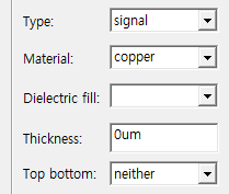
1691109608890.png


I checked that the '.tf' file provided by TSMC also has no thickness information.

The pdk only shows the thickness information of M1-M5.

I need to know the thickness of the via between M1-M5 so that I can enter the thickness information in hfss properly.

If anyone knows how to do this, please help me.

Thanks.
 
In processes with CMP (chemical-mechanical polishing, to
get planarity for the next layer) on the dielectrics, the
dielectric layer thickness becomes variable by location /
underlying topography. On stacks taller than about 3
levels and below maybe 250nm this is very common.
Too much Z variation messes with finer-litho depth of field
and ability to control dimensions (defocusing leads to
variation and that could get ugly, gone too far).


If you're lucky you might find a cartoon of cross section
and maybe down in the modeling docs, some disclosure
of ILD thicknesses (look for parasitic capacitance extract
rules, and any "MOM cap" modeling). But don't expect
great accuracy.


A SEM cross-section of the stack above a representative
"device layer" (what are you sitting above, and how lumpy
does that make your cushion?) would be informative, and
published papers involving your target technology might
be found. Or maybe your efforts can be aimed at a layout
with only clear field below, which might have better odds
of appearing in foundry interconnect-stack documentation
(or just a fortunate stray pic).
 

LaTeX Commands Quick-Menu:

Part and Inventory Search

Welcome to EDABoard.com

Sponsor

Back
Top