Continue to Site

Welcome to EDAboard.com

Welcome to our site! EDAboard.com is an international Electronics Discussion Forum focused on EDA software, circuits, schematics, books, theory, papers, asic, pld, 8051, DSP, Network, RF, Analog Design, PCB, Service Manuals... and a whole lot more! To participate you need to register. Registration is free. Click here to register now.

Biasing a MOSFET changes input signal

Status
Not open for further replies.

I14R10

Full Member level 3
Joined
May 31, 2015
Messages
185
Helped
0
Reputation
0
Reaction score
0
Trophy points
1,296
Activity points
2,750
First of all, I will say I only have basics of analog electronics, so my design is probably wrong in so many places.

What I'm trying to do:
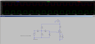
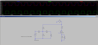
I have a square wave, but not from -V to +V, instead from 0 to V.
Next step, C1, R1 remove DC component of the signal
R2, C2 make low pass filter that gets me a triangle wave.

At this point, without the rest of the circuit to the right, I have an amplitude of around -0.4V to +0.4V at the junction of R2 and C2.
Now I want to amplify that signal with a MOSFET. MOSFET alone doesn't change my signal, but when I bias it to get a half of 5V on drain, those resistors for biasing lower the signal on the junction of R2, C2 and C4. What can I do to completely separate those two circuits so that I can bias MOSFET properly?
--- Updated ---

If I put an opamp as a buffer, things work. But let's say I don't want to use op Amps, how would I do it?
 

Attachments

  • Screenshot_20220616_114050.png
    Screenshot_20220616_114050.png
    41.5 KB · Views: 112
  • Screenshot_20220616_123028.png
    Screenshot_20220616_123028.png
    41.2 KB · Views: 105
Last edited:

You can omit C4 and replace R1 by a bias voltage divider.
You mean like this?
Still the same thing happens.

Green is voltage source, red is junction of R7 and R1, blue is R2-C2 junction.
 

Attachments

  • Screenshot_20220616_131201-1.png
    Screenshot_20220616_131201-1.png
    34.7 KB · Views: 93
  • Screenshot_20220616_131445.png
    Screenshot_20220616_131445.png
    36.2 KB · Views: 91

Don't know what you mean. There's no signal magnitude reduction visible in the waveform, still about 0.8 Vpp.

You may want to make the impedance of the bias network equal to 100k of the first circuit, for some reason you reduced it now. You should also consider that the amplifier input capacitance adds to the low pass capacitor, the effect has nothing to do with bias network.
--- Updated ---

To overcome the latter effect, R2 (and possibly also C1) need to be scaled respectively.
 
Last edited:

Don't know what you mean. There's no signal magnitude reduction visible in the waveform, still about 0.8 Vpp.

You may want to make the impedance of the bias network equal to 100k of the first circuit, for some reason you reduced it now. You should also consider that the amplifier input capacitance adds to the low pass capacitor.

Blue waveform is the one that I'm interested in. Peak to peak voltage is lower when it's connected to the MOSFET.


R1 remained 100k, and I lowered R7 value to get the right ratio for biasing.


Ah, yes, I forgot about the MOSFET gate capacitance. I'l go play around with that.
 

Hi,

Could a JFET (high input impedance) between R2C2 (C4) and the MOSFET replace the OA? Or would that just make matters worse, or be throwing unnecessary components at the problem? 2N5457 could match voltages you are using and is so common, LTSpice must have the model. Not sure/very convinced how 'off' a JFET would be at only -0.4Vgs.

It works. But think op amp still wins regarding how easy it is to implement.

Why does JFET work but MOSFET doesn't? Gate capacitance?
 
Last edited:

Hi,

Really? Great, I'm glad to hear it.

My guess is extremely different order of magnitude of gate resistance between MOSFET and JFET. I just did '(extremely, but seriously) bad, quick maths' from BSS145 datasheet, it doesn't say what Rgate is but for certain conditions, 18ns turn-on time/80pF input capacitance = 225R... Probably wrong value but the calculation shows how JFETs are used for their high input impedance.

Glad it might work, and yes, I agree - OAs are super as buffers that bring few problems in comparison.
 

Status
Not open for further replies.

Part and Inventory Search

Welcome to EDABoard.com

Sponsor

Back
Top