helenpenghan
Newbie level 4
Can anyone offer me any hints on the design of differential buffer stage and bias circuit? I have read the "Low-jitter process-independend DLL and PLL based on self-biased techniques", but I still get confused about some issues. Actually, I am trying to design a DLL for which can generate phase delayed clock signal ( up to 200MHz) and varing duty cycles. I would like to have low jitter performance.
However, when I am simulating with the differential buffer delay stage, I found the differential output is not rail-to-rail, actually the control signal determines the ouput lowever level. If it is not rail-to-rail, how to connect to next delay cell? I will need at least 4 stages? And, since the input and output are differential signals, do I need to put any single-end to differential circuit before and after the delay cells?
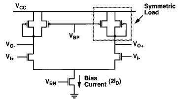
Thank you very much. I attached the exact circuit I am using from that paper.
However, when I am simulating with the differential buffer delay stage, I found the differential output is not rail-to-rail, actually the control signal determines the ouput lowever level. If it is not rail-to-rail, how to connect to next delay cell? I will need at least 4 stages? And, since the input and output are differential signals, do I need to put any single-end to differential circuit before and after the delay cells?
Thank you very much. I attached the exact circuit I am using from that paper.