Continue to Site

Welcome to EDAboard.com

Welcome to our site! EDAboard.com is an international Electronics Discussion Forum focused on EDA software, circuits, schematics, books, theory, papers, asic, pld, 8051, DSP, Network, RF, Analog Design, PCB, Service Manuals... and a whole lot more! To participate you need to register. Registration is free. Click here to register now.

BGA Breakout routing for impedance-controlled board

Status
Not open for further replies.

nelsonys

Member level 4
Joined
May 23, 2011
Messages
77
Helped
8
Reputation
16
Reaction score
8
Trophy points
1,288
Activity points
2,034
I have come across Intel board design which is designed in a rather confusing way.
Sorry it's a classified document which I'm not able to show it here and I'll try my best
to explain in words.

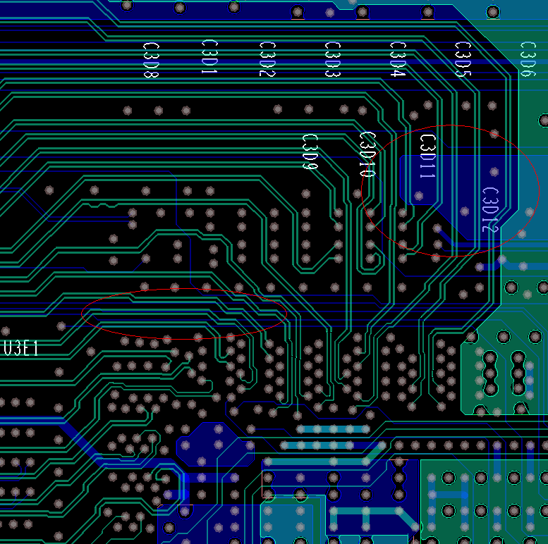
The PCB designers of Intel squeezed 4-5 traces in between breakout pins from BGA.
These traces need deskewing using serpentine routing before reaching the connector.
One thing confused me is that the board are well impedance controlled, but the trace
width themselves varied from portion to portion.

Say from breakout, the width is 0.1mm, after passing breakouts pins the width changes
to say, 0.15mm with wider clearance in between each traces.

Questions are:
1) Do they need to consider the strong coupling between traces at the breakout portion?
2) How did they manage to control the impedance to 50ohm by having two trace width?
3) Weird stackup by having two signal layers (even though contains differential signals)
sandwiched in between Power layers.

Besides, I would like to ask for opinion regarding inductor layout for power supply.
I come across a board design with the portion of the power layers (GND and VCC) under
the inductor being deliberately removed for the sake of EMC measures.
From my understanding, if there's no direct return under the inductor, it might as well
radiates EM field to the outer world isn't it??

Thanks,
Nelson
 

Firstly Inductors and power supplies, it is reccomended for best EMC and noise results to remove ALL copper from under SMPS inductor and switching traces. So as well as the inductor remove copper from under the switching loops. As illustrated below.
As to the layout, only simulation and field solvers will answer the question without ambiguity. My view, with 4 layers cost was an important factor. What we have to remember is that even bad designs will work, not as well as a good design and more likely to fall over at temperature extremes. But at normal temperatures under normal conditions they will work, with possible problems and extra latency etc.
 

Attachments

  • 5Vpsu-gnd.bmp
    3.6 MB · Views: 68
  • 5Vpsu-top.bmp
    3.6 MB · Views: 52
  • 5Vpsu-pwr.bmp
    3.6 MB · Views: 62

So as well as the inductor remove copper from under the switching loops.
I can't agree if you consider it as a general suggestion. Ground plane under the switching loop basically reduces it's inductance and may be wanted for better switching behaviour. In so far it's at least a trade-off. Ground under inductors ... depends on the inductor design, I suppose.

You want of course to keep switched currents inside the SMPS area and particularly avoid leaking into ground plane. There are different means to achieve. it.

For the impedance controlled layout questions, I agree with marce that you should avoid jumping into coclusions. Asking "how did they achieve" assumes that they did. But you can't know, except for the fact that the design has been apparently working.
 

Sorry, but I have to disagree, this information comes from one of the top people in SMPS design who worked for Linear, then National and now works for Ti since they took over National. It is also information I have been given by other switcher application engineers. Since he's quite high up in SMPS design and EMC problems that result I would say that what he reccomends be taken quite seriously.
Capacitive coupling is the problem with copper under the switching nodes, so as the experts say dont put copper under switching nodes of SMPS. The switching ground for your switchers should all be on the component layer and joined at the minimum number of points to reduce circulating currents on actual ground planes. The actual ground plane should not be involved with the switcher in any active way, a seperate switche ground should be used to contain the switching ground currents.
You will also notice from the attached example that just the right amount of copper is used especially around the input and output capacitors, not to much not to little.
 

As said, there are different means to achieve the EMC objectives. I didn't say, the void suggestion is wrong, but there are concurrent aspects, thus I doubt it's general validity. Capacitive coupling is an important point, but injected currents can be drained by an additional local power ground plane (layer I2N) below the switcher. It's also preferable as low inductance return path for input/output capacitors.
 

Thanks both Marce and FvM!

I came across a book from Intel that for PCIe, they did not explicitly required a certain impedance for the trace, and they mentioned as long as the differential trace stay in 100ohm +- 20%, it would give correct outcome. Forgive me for my ignorant, isn't this statement kind of vague? How to get an impedance by not using the usual microstrip or stripline configuration?
I do understand that as long as the eye pattern yields acceptable result within margin, the impedance doesn't matter at all for PCIe.

For the attached pic, I found that the planes below is cut nicely according to the dimension of the main switching route. Do we have to consider the fringe of field that may possibly couple to the GND plane too?

---------- Post added at 09:43 ---------- Previous post was at 09:06 ----------

"Dual stripline — in this case the two signal conductors are sandwiched between the two reference planes on adjacent layers. These two signal layers will be routed orthogonally to minimise inter-layer crosstalk; i.e. the signal layers are made to cross at right angles so as to minimise the crossing area. The structure is then behaving as two independent offset striplines." as quoted from Polar Instruments.

This is the image for the differential pairs of PCIe on L4 which you can find that some of the differential pairs overlap with the traces or even plane on L3. In fact other single-ended lines also overlap with the plane at L3 for a quite long distance, 2cm above.
Eventually, eye pattern decides whether this routing methodology is feasible or not, I guess...
 

There is another technique where you can create a isolated ground section under the switching node (for anyone following this, we are debating this node; that has has the highest dV/dt in the switcher, hence its importance for noise). Connecting this to the main ground at one point, but for small switchers especiaqlly whenthey are cascaded on a digital board, the simplest and best results fo far have been to clear copper under this node. The switching node should be very very small area anyway.
The seperate ground part is in a couple of app notes, I'll dig them out, but the idea is similar to capacitive screening in planar transformers.
Again most switcher app notes do reccomend keeping the switching ground, incluing IO capaciotr grounds on one layer and connecting this down to system ground planes at one point (with multiple vias).
 

Status
Not open for further replies.

Part and Inventory Search

Welcome to EDABoard.com

Sponsor

Back
Top