Continue to Site

Welcome to EDAboard.com

Welcome to our site! EDAboard.com is an international Electronics Discussion Forum focused on EDA software, circuits, schematics, books, theory, papers, asic, pld, 8051, DSP, Network, RF, Analog Design, PCB, Service Manuals... and a whole lot more! To participate you need to register. Registration is free. Click here to register now.

[SOLVED] Avalanche Pulse Generator

Status
Not open for further replies.

PlanarMetamaterials

Advanced Member level 4
Joined
Jun 13, 2012
Messages
1,456
Helped
404
Reputation
812
Reaction score
382
Trophy points
1,363
Location
Edmonton, Canada
Activity points
9,824
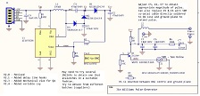
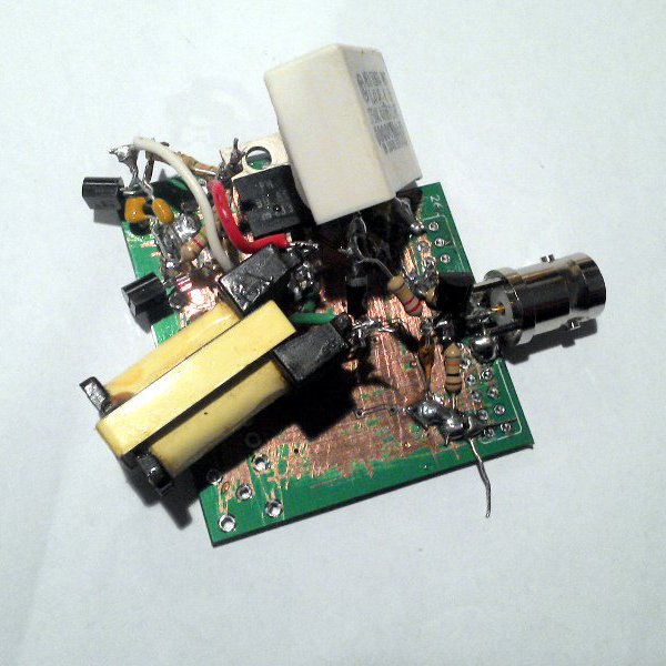
I'm new to electronics and am trying to design a sub-nanosecond 50V pulse generator via an avalanche transistor. I've chosen Zetex's FMMT413 transistor as it looks perfect for the task. I designed the following circuit:

1655307148804.png


Which, as far as I can tell, is pretty standard.

However, I cannot get this circuit to produce an output (I'm using a 5 GHz scope connected to Vout). I've tried adjusting Vin from 60V to 120V, and applied a square wave input to the trigger. As far as I can tell, all the components are working properly and I've measured proper voltages at every node. I've tried three different transistors just in case, and have tried replacing C11 with a 5 nF cap as per the datasheet and application note. The variable resistor R6 is maxed at 100 kOhm, adjusting to a lower value doesn't make a difference.

Any suggestions as to how to obtain the desired output?
 

Solution
Aright, thanks everyone for your input.

betwixt and FvM take the proverbial cake for providing the correct answer -- depending on the mode.

Firstly, I replaced the SM2 with a more standard RCP0603W50R0GEB.

To obtain a triggered avalanche response, I pulsed the trigger input with a +/- 5V square wave at 1 kHz. The output could be observed sharply transitioning between follower mode and avalanche mode when the supply voltage Vin exceeded 85V. I suppose this is inline with the datasheet curves for the give dI/dt at the base.

I was also able to obtain the desired "free-running" mode by obtaining another power supply and increasing the supply voltage substantially. Avalanching was observed in the absence of a trigger pulse when the...
Hi,

You should post a photo of the test set-up and of the oscilloscope results, if you can. You don't say Vout expected. Easier for people to assess issue with images.

I read a bit about these circuits after another member asked about them recently, and they look very hard to get to work. Some I saw used 2N3904.

I decided to simulate a similar circuit, with and without trace/wire effects of R, L and C - you can guess which version had awful results.

Out of curiosity, do you think using the CR on the base as the output pulse by taking it off the base, and driving the BJT from the same input pulse to pull output low has potential to work or is that a stupid idea? CR will rise and fall much faster (at that speed, 'square' wave appears to be descriptive more than what the actual output waveform is), and BJT might have started to turn on enough to drain any residual voltage. I'll show a picture of what I mean later or tomorrow.
--- Updated ---

... don't laugh too much, it's probably a really stupid idea (which is why no-one does it this way), this kind of circuit is well beyond my ability. I used a GaN transistor model because they are supposed to be very fast devices. The wire model was copied from one of two I found, no idea how accurate it is and I exaggerated R, L and C in it. I later found that C2 (C4) is completely and utterly unnecessary. ~1.2V out for ~500ps and ~100ps rise and fall times as those were the other person's design goals.

PULSE THING 2.JPG


PULSE THING 2 full.JPG


Maybe your issue is related to wiring and lead capacitance?
 
Last edited:
You should post a photo of the test set-up and of the oscilloscope results, if you can. You don't say Vout expected. Easier for people to assess issue with images.

Sure, here's a pic of the relevant layout. The RF chain is C11->J3.

My expected Vout is Vout > 0 Volts :) Ideally this would be a "free-running" pulse generator that continuously generates pulses, and triggering wouldn't be required. This type of output is detailed in the second plot here.

Without a trigger, there's literally nothing to see on the scope; as the transistor isn't avalanching it's a flat line at 0 volts.

1655327247523.jpeg


I read a bit about these circuits after another member asked about them recently, and they look very hard to get to work. Some I saw used 2N3904.

The sources I've read seem to make these designs seem really easy, since exact values aren't required -- so long as the source voltage is large enough. It seems 2N series transistors are very common in avalanche pulsers, yes. But as I understand it, those transistors aren't necessarily designed to avalanche, whereas the FMMT41X series are, so I figured they would be the way to go.

I decided to simulate a similar circuit, with and without trace/wire effects of R, L and C - you can guess which version had awful results.

I'm not too worried about my layout at this point, just trying to get any shape of pulses out.

Out of curiosity, do you think using the CR on the base as the output pulse by taking it off the base, and driving the BJT from the same input pulse to pull output low has potential to work or is that a stupid idea? CR will rise and fall much faster (at that speed, 'square' wave appears to be descriptive more than what the actual output waveform is), and BJT might have started to turn on enough to drain any residual voltage. I'll show a picture of what I mean later or tomorrow.

... don't laugh too much, it's probably a really stupid idea (which is why no-one does it this way), this kind of circuit is well beyond my ability. I used a GaN transistor model because they are supposed to be very fast devices. The wire model was copied from one of two I found, no idea how accurate it is and I exaggerated R, L and C in it. I later found that C2 (C4) is completely and utterly unnecessary. ~1.2V out for ~500ps and ~100ps rise and fall times as those were the other person's design goals.
I'm not too familiar with other possible topologies [this is my first electronics design project in over a decade]; but I do want to keep the avalanche behavior for voltages > 50V.

Thanks!
 
Last edited:

Hi,

Thanks. Nice PCB, really tidy. I'll look at the transistor's datasheet tomorrow. I won't be able to help much but I'll try if I can.

One approach could be to measure/capture current going into transistor or into 50R, if you haven't already tried that.

Another, if you're okay with it, do you have a (copy/paste here or photo of notepad to save you time) of how you worked out the component values for expected output time(s), voltage, (etc. if anything else)? From there, comparing calculated results to obtained results might help give a clue to cause of 0Vout.

You don't seem the kind of person to forget a wire or suchlike or have an oscilloscope that is, or is just set, too slow compared to signal, etc. so test set-up must be correct.

What is source impedance/resistance, do you know?
 

It should at very least work as an emitter follower but my guess is you need more voltage to reach avalanche condition. Probably in excess of 150V.

Brian.
 

    d123

    Points: 2
    Helpful Answer Positive Rating

    PlanarMetamaterials

    Points: 2
    Helpful Answer Positive Rating
Thanks. Nice PCB, really tidy. I'll look at the transistor's datasheet tomorrow. I won't be able to help much but I'll try if I can.

Thanks for looking regardless.

One approach could be to measure/capture current going into transistor or into 50R, if you haven't already tried that.
I've used a high-impedance probe to look at the voltage on the output; since there's no voltage I think it's safe to say there's no current there.

Another, if you're okay with it, do you have a (copy/paste here or photo of notepad to save you time) of how you worked out the component values for expected output time(s), voltage, (etc. if anything else)? From there, comparing calculated results to obtained results might help give a clue to cause of 0Vout.
This is actually my evaluation circuit for obtaining the (rough) pulsing properties of the transistor -- since I couldn't model it, I have no idea what to expect in terms of pulse performance. I plan to play around with the components... once I get it pulsing.

You don't seem the kind of person to forget a wire or suchlike or have an oscilloscope that is, or is just set, too slow compared to signal, etc. so test set-up must be correct.
Thanks, I'm pretty sure I've double-checked everything else.
What is source impedance/resistance, do you know?
Very low, I have a nice benchtop power supply, so I don't think this is an issue. I expect a large charge time anyways with the 100kOhm source resistance.
--- Updated ---

It should at very least work as an emitter follower but my guess is you need more voltage to reach avalanche condition. Probably in excess of 150V.
I was hoping this wouldn't be the case -- my power supply only goes up to 120V. The datasheet gives Vceo at 50V -- wouldn't this be the relevant parameter here? I see that Vcbo is 150V but I'm not trying to initiate the avalanche from the base. I guess I'm not sure what Vces is and how it differs from Vceo.
 
Last edited:

I agree that using a transistor with specified avalanche behaviour should be advantageous. When I designed avalanche pulsers 35 years ago, we didn't have such devices.

You didn't give any information about the trigger generator and its waveform. Datasheet tells about a alanche operation with 4n7 capacitance starting at about 60 V, however with trigger dI/dt of 5 mA/ns.

The 50R resistor SM2 is wirewound and hardly suited for high speed pulse applications. Nevertheless the 50R oscillloscope input impedance should be a suitable load, at least in principle. I'm not sure if the oscilloscope input has sufficient voltage rating.

Regarding simulation of avalanche operation, I won't expect that second breakdown is modelled by standard SPICE transistor model.
 

    d123

    Points: 2
    Helpful Answer Positive Rating

    PlanarMetamaterials

    Points: 2
    Helpful Answer Positive Rating
You didn't give any information about the trigger generator and its waveform. Datasheet tells about a alanche operation with 4n7 capacitance starting at about 60 V, however with trigger dI/dt of 5 mA/ns.
Hmm, thanks, I didn't actually connect this value with the trigger pulse. Do you think this means that the device can't operate in "free-run" mode where there is no trigger, and dI/dt = 0?

The 50R resistor SM2 is wirewound and hardly suited for high speed pulse applications.
Thanks for pointing that out.

I'm not sure if the oscilloscope input has sufficient voltage rating.
Thankfully, I am :) But thanks for pointing it out, as well. It's a great scope and it would be a shame to lose a channel or two.
 

So I guess the operating mode is a snapback triggered
by normal conduction? It's then important that a device
be selected, which actually has a snapback behavior.
Well designed ones would not. Or, they'd be rated below
where this mechanism could be provoked. You're looking
for a parameter which won't appear, except roundabout,
on a datasheet.

What voltage output are you looking for? The 100K/50
division is the max you can get, pulse width (if triggered
into a latched state) will persist for the C11*50 ohm time
constant.

If you want free running narrow pulses I might suggest a
logic based pulser, one which puts out a 1-gate-delay
"yip!" on every rising edge could be had with a quad
NAND gate and some of the low voltage logic familes
can approach 1ns delays; you could also consider ECL
for a 50-ohm-friendly, sub-ns logic family.

Consider that even with a 500MHz 'scope channel BW,
your "1nS" pulse is 4X the required BW (if you figure
that a "pulse" must at minimum be represented by
tr and tf at full power BW, 500ps/500ps and I say
500ps needs a 2GHz BW to display even a roughly
right waveshape. Might want to debug at a wider
pulse width initially (if indeed the chosen transistor,
delivers the desired "abnormal behavior").
 
  • Like
Reactions: d123

    d123

    Points: 2
    Helpful Answer Positive Rating
Scope risetime DIY pulse generators in the PS area -


Regards, Dana.
 

Aright, thanks everyone for your input.

betwixt and FvM take the proverbial cake for providing the correct answer -- depending on the mode.

Firstly, I replaced the SM2 with a more standard RCP0603W50R0GEB.

To obtain a triggered avalanche response, I pulsed the trigger input with a +/- 5V square wave at 1 kHz. The output could be observed sharply transitioning between follower mode and avalanche mode when the supply voltage Vin exceeded 85V. I suppose this is inline with the datasheet curves for the give dI/dt at the base.

I was also able to obtain the desired "free-running" mode by obtaining another power supply and increasing the supply voltage substantially. Avalanching was observed in the absence of a trigger pulse when the supply voltage was increased past 170V.

dick_freebird is correct that the pulse is drawn out due to C11*R7; what I was looking for was a fast-rising edge, so the drawn out discharge (~500ns) isn't an issue for me.

In the end, the voltages are a bit larger than what I was hoping for with this transistor, but they are manageable.
 
Solution
Status
Not open for further replies.

Similar threads

Part and Inventory Search

Welcome to EDABoard.com

Sponsor

Back
Top