Continue to Site

Welcome to EDAboard.com

Welcome to our site! EDAboard.com is an international Electronics Discussion Forum focused on EDA software, circuits, schematics, books, theory, papers, asic, pld, 8051, DSP, Network, RF, Analog Design, PCB, Service Manuals... and a whole lot more! To participate you need to register. Registration is free. Click here to register now.

Audio Circuit - Unstable Amplifier

Status
Not open for further replies.

gujjubhai123

Newbie level 4
Joined
May 15, 2009
Messages
7
Helped
0
Reputation
0
Reaction score
0
Trophy points
1,281
Location
USA
Activity points
1,408
hello,

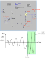
I have build this amplifier. In lab, I am applying 10mV rms at the input. At output I see 400mV-rms at time=0s. And over 3.5minutes, the output rises from 400mV-rms to 500mV-rms. The expected output is 500mV-rms. After the output crosses say 504mV, the amplifier becomes UNSTABLE.

I plotted loopgain vs frequency. When dB(LG) crosses 0dB, the phase(LG) has passed by 180deg w.r.t. the starting phase of 90deg at 1mHz. Do you agree with that assessment that this amplifier with such a LG is unstable? "LG" is the probe inserted in the outer loop.

What's causing the 3.5minute transient?

Your input is greatly appreciated!

Loopgain method: "LG" developed by (c) Sandro Herrera, SW Audio.
[1] Michael Tian, V. Visvanathan, Jeffrey Hantgan, and Kenneth Kundert,
"Striving for Small-Signal Stability", IEEE Circuits and Devices Magazine,
vol. 17, no. 1, pp. 31-41, January 2001.
audio_amplifier_unstable.png
 

Hi,

this all makes no sense.

I am applying 10mV rms at the input. At output I see 400mV-rms
at which frequency?

at time=0s. And over 3.5minutes, the output rises from 400mV-rms to 500mV-rms.
where can we see this?

The expected output is 500mV-rms.
Why?

What's causing the 3.5minute transient?
We can´t see a "3.5 minute transient" (in the time domain).
Transients are usually fast (below microseconds), but "minutes" are so slow that it is not of interest when one talks about "audio".

Is the plotted gain:
* open loop
* or closed loop?

We can´t see what OPAMP you used.

The values for C2, C3 and R3, R5 make no sense (in my eyes) for an audio circuit.

Why the JFET input at all?

Klaus
 

There are some absurd component values on your schematic. For instance 1mF-10 Ohm, 5 MOhm-10pF..
These values are unusual and may create trouble.( Simulator may also not converge ).
Simulators don't like such absurd values, correct them ( by well calculation ).
 
"Normally" one thinks of transients in the second to minute area for power
devices impacting thermal stability control loops inside parts, like regulators.

Or an amp oscillating in RF region developing a lot of power.....

Sounds like this is not in the sim, but bench testing ?

What is part number of amp ?

You using JFET because actual input is for electret mics ?


Regards, Dana.
 

Hi,

this all makes no sense.


at which frequency?


where can we see this?


Why?


We can´t see a "3.5 minute transient" (in the time domain).
Transients are usually fast (below microseconds), but "minutes" are so slow that it is not of interest when one talks about "audio".

Is the plotted gain:
* open loop
* or closed loop?

We can´t see what OPAMP you used.

The values for C2, C3 and R3, R5 make no sense (in my eyes) for an audio circuit.

Why the JFET input at all?

Klaus

Klaus,

Q) this all makes no sense.
=> my apologies. let me attempt round two.

Q) at which frequency?
=> At 1kHz. Basically I inject 10mV-rms 1kHz since wave at the JFET input and observe Vout = 500mV-rms at the output. Gain being = 1+Rf/Rs = 50V/V = 34.15dB.

Upon power up, the output is ~420mV-rms and slowly the output amplitude starts increasing over ~3.5minutes, until the output reaches ~504mV-rms. This is when the amplifier goes unstable. The output turns into 1.3MHz, -2V to 2V triangular shape wave.

Q) where can we see this?
=> I have annotated the original diagram with where the input and outputs are.

Q) Is the plotted gain:
* open loop
* or closed loop?

=> what's plotted is Loop-gain = feedback_factor_beta * Open_loop as a function of frequency. This was my attempt. In Cadence spectre, there exists a stability probe used with STB analysis. In LTSPICE, I am using the same approach using the Tian method (instead of Middlebrook) for loop-gain analysis for stability assessment.

Q) We can´t see what OPAMP you used.
AD743. I am using the malromodel provided by ADI.

Q) The values for C2, C3 and R3, R5 make no sense (in my eyes) for an audio circuit.
=> original concept is inspired by : https://www.planetanalog.com/amplify-small-signals-in-low-noise-circuit-with-discrete-jfet/

Q) Why the JFET input at all?
I have a MEMS capacitive transducer that generates signals. The input-referred capacitance attenuates the signal. This JFET has least amount of capacitance, from it's PN-junction.

I have added transients (manually drawn) for illustrations below.
 

Attachments

  • audio_amplifier_unstable_legends.png
    audio_amplifier_unstable_legends.png
    163.1 KB · Views: 112
Last edited:

"Normally" one thinks of transients in the second to minute area for power
devices impacting thermal stability control loops inside parts, like regulators.

Or an amp oscillating in RF region developing a lot of power.....

Sounds like this is not in the sim, but bench testing ?

What is part number of amp ?

You using JFET because actual input is for electret mics ?


Regards, Dana.

hi dana,

Q) Sounds like this is not in the sim, but bench testing ?
=> Yes, not in simulations, but bench testing.

Q) What is part number of amp ?
=> AD743

Q) You using JFET because actual input is for electret mics ?
=> The sensor is a capacitive MEMS transducer. The capacitance at MEMS:AFE interface needs to be minimized, to minimize the signal loss. In other words, the lower the MEMS:AFE capacitance, larger the signal.
 

Hi,

For me: neither 2V amplitude, nor 1.35MHz makes sense. There must be something "besides" the schematic...

May we see a photo of your circuit? (~100kBytes)

Where exactly did you connect the scope probe (2 connections)
Does it oscillate even if the scope is not connected?
Do you use a solid GND plane?
Do you use proper bypassing the power supplies of the OPAMP and the FET?

Klaus
 

Drift and distortion like that can only be from thermal effects and heating can only come from instability.
Component layout and wiring is critical, in fact I would go so far as to suggest that the FET doesn't do anything useful that good layout wouldn't do better.

Brian.
 

In just the amp with the 190 pf load I do not see a lot of phase margin as I range R3 from 1k - 10k:

1661971775948.png


And it occurs a little over 1 Mhz.

I also noticed in datasheet C load characterization a tad thin. One diagram with 100 pF,
no other comments.


Regards, Dana
 
Last edited:

It's not clearly stated, but I expect that slow magnitude rise is caused by the sensor input, not amplifier gain drift. If so, the problem under discussion is "why amplifier falls into oscillations above a certain signal level"?

Large signal instability is usually caused by nonlinear circuit properties, e.g. OP slew rate or output current limits. It can't be seen in small signal loop gain analysis. In the shown circuit, the high capacitive load may be sufficient to cause such effects.

If you want us to analyze circuit details you should zip LTspice .asc file together with nonstandard library files.
 

In just the amp with the 190 pf load I do not see a lot of phase margin as I range R3 from 1k - 10k:

View attachment 178325

And it occurs a little over 1 Mhz.

I also noticed in datasheet C load characterization a tad thin. One diagram with 100 pF,
no other comments.


Regards, Dana
Thank you Dana, for going through the effort of simulating the PM. I appreciate it.

I have switched to a different topology, which is simpler and stable.
--- Updated ---

It's not clearly stated, but I expect that slow magnitude rise is caused by the sensor input, not amplifier gain drift. If so, the problem under discussion is "why amplifier falls into oscillations above a certain signal level"?

Large signal instability is usually caused by nonlinear circuit properties, e.g. OP slew rate or output current limits. It can't be seen in small signal loop gain analysis. In the shown circuit, the high capacitive load may be sufficient to cause such effects.

If you want us to analyze circuit details you should zip LTspice .asc file together with nonstandard library files.
Hi FwM,

thanks for sharing. it's possible, but in this case, I have a sine-wave driver 10mV-rms from a function generator.
 

Status
Not open for further replies.

Similar threads

Part and Inventory Search

Welcome to EDABoard.com

Sponsor

Back
Top