Welcome to our site! EDAboard.com is an international Electronics Discussion Forum focused on EDA software, circuits, schematics, books, theory, papers, asic, pld, 8051, DSP, Network, RF, Analog Design, PCB, Service Manuals... and a whole lot more! To participate you need to register. Registration is free. Click here to register now.
The entire device can be erased at one time by using a 6-byte software code.
The software chip erase code consists of 6-byte load commands to specific address locations with specific data patterns.
Once the code has been entered, the device will set each byte to the high state (FFH). After the software chip erase has been initiated, the device will internally time the erase operation so that no external clocks are required.
The maximum time required to erase the whole chip is tEC (20 ms). The software data protection is still enabled even after the software chip erase is performed. If the boot block lockout feature has been enabled, the 6-byte software chip erase algorithm will not function.
Take a look at this file for the detail algorithm to do chip erase
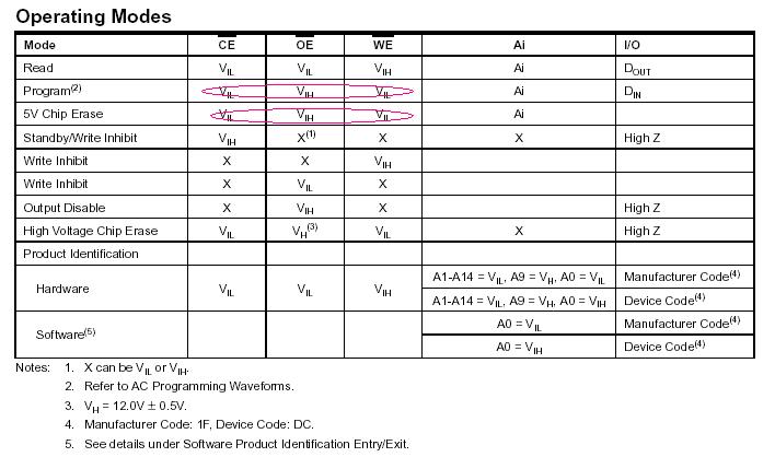
From hardware point of view, Program and Erase is a same process, ie write data to the chip, so /CE=0 (chip selected), /OE = 1 (disable trisate output buffer), /WE = 0 (it is a write process)
But Chip Erase is very special write process, write special 6 bytes code to different location as mention in the Application note. Write special code to special location with certain sequence make the chip recognize it is chip erase mode not prgram mode
This site uses cookies to help personalise content, tailor your experience and to keep you logged in if you register.
By continuing to use this site, you are consenting to our use of cookies.