Continue to Site

Welcome to EDAboard.com

Welcome to our site! EDAboard.com is an international Electronics Discussion Forum focused on EDA software, circuits, schematics, books, theory, papers, asic, pld, 8051, DSP, Network, RF, Analog Design, PCB, Service Manuals... and a whole lot more! To participate you need to register. Registration is free. Click here to register now.

[SOLVED] Arrangement of isolated variable DC input

Status
Not open for further replies.

mkeyno

Newbie level 5
Joined
Mar 8, 2024
Messages
9
Helped
0
Reputation
0
Reaction score
0
Trophy points
1
Activity points
98
I design isolated DC input for industrial applications that can possibly work from 12 to 24 V.


I add a 5.1 V Zener for over-voltage protection, a capacitor for filtering, and TVS for surge production.


My questions are:


In an overvoltage situation, will any LED light turn on?


Is this the correct arrangement of elements? Can I switch the position for the Zener and capacitor?
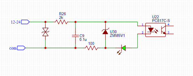
1709935673532.png
 

Provided 'com' is the negative side of the supply it will work but put the 100R resistor between U30 and the cathode of the green LED and link across its present position. At the moment it is the green LED and the LED inside U22 that clamp the voltage, not the Zener diode.

Note that the TVS only provides protection by dumping current from the supply. It probably isn't necessary at all but if you keep it you should either add a fuse or resistor in series with the input to protect against it drawing excessive current.

Brian.
 

thanks Brian
Provided 'com' is the negative side of the supply it will work but put the 100R resistor between U30 and the cathode of the green LED and link across its present position. At the moment it is the green LED and the LED inside U22 that clamp the voltage, not the Zener diode.

Note that the TVS only provides protection by dumping current from the supply. It probably isn't necessary at all but if you keep it you should either add a fuse or resistor in series with the input to protect against it drawing excessive current.

Brian.

the purpose of this design is to protect the input signal in harsh industrial environments, and I assumed the TVS is the first layer and the Zener Diode is the last layer of protection and green LED could be useful to know if the input port destroys
do you believe the following designs have more advantages?


1709937085997.png
 

I design isolated DC input for industrial applications
A proper design starts with requirements / specicfications.
* ON current, ON voltage
* OFF voltage, OFF current
* operating frequency
* may delay time
* erroneous (noise, wrongly wired ....) signals in value, polarity, duration
* behaviour (on error)

In an overvoltage situation, will any LED light turn on?
This is rather basic. As an industrial electronics designer you should: either know or demand how your circuit should behave.

Is this the correct arrangement of elements? Can I switch the position for the Zener and capacitor?
Also rather basic.
I wonder what is your level of knowledge. Before it seemed you are an experienced designer. But maybe you are a newbie.

For a newbie I strongly recommend to use simulation software. There you simply can force situations and look at the behaviour without the risk for smoke and explosion.
There is free and easy to use simulation software.

the purpose of this design is to protect the input signal in harsh industrial environments, and I assumed the TVS is the first layer and the Zener Diode is the last layer of protection and green LED could be useful to know if the input port destroys
do you believe the following designs have more advantages?
No, you don´t want to protext the input signal. You rather want to protect the circuit, the electronic parts.
But for this you first need to define the "normal conditions" and the "overvoltage conditions".
One needs to know how much voltage / current for how long time is "normal" and the circuit should work without properly.
To protect against 30V is rather easy, to protect against a 2000V ESD pulse is rather easy, to protect against 230V (AC or DC, caused by wrong wiring) is rather difficult.
--> It´s not only the voltage, but also the duration and the energy and power dissipation that defines how to design (calculate) the protecion circuit.

***
Your circuits of post#3:
I wonder if "COM" is really a single commoon node for several inputs (then call it GND, or input_GND or similar and use an according GND_symbol)
..or are they individual nodes for each input? (Then don´t call them "COM" = common. Better call them IN1-, IN2-, IN3-...)

The first circuit is "critical", because the forward voltage of the (unknown) LED defines the input threshold. So if you use a red LED you input threshold will be different to a using blue LED.

The second circuit .. zener diode protection for positive input voltage does not work at all.

and green LED could be useful to know if the input port destroys
So it´s a green LED. And it should show when the input is destroyed? Or did I misunderstand?

do you believe the following designs have more advantages?
More advantages "regarding what"? positive overvoltage protection level, negative voltage protection level, switching thresholds, speed, power dissipation, cost, area, ....)

Maybe you can´t give exact values for all this. But you need to be "aware" of this. And clearly state what / how you expect your circuit to work.

"can possibly work from 12 to 24 V." .. Does this mean if the input signal is below 12V (like 11.9V) then it´s allowed for the output to become LOW?
Or does 12V...24V rather describe the power supply for PLC systems (where for example the signal switching voltage thresholds are "<3V for LOW" and ">6V for HIGH")

Industrial DC inputs exist since decades. Why do you try to re-invent the wheel (while I have doubts about YOUR requirements, the specifications and the skills).
Thus I simply ask myself "Why?"
Why not refer to standards, standard operation conditions, standard error conditions, standard circuits?
It should be an easy task to opean a SIEMENS PLC datasheet (for example) to see the conditions / requirements / protection levels, maybe even the input circuits...
(and you can be sure it is proven billion times and for decades already) At least it gives a lot of information about what to care for, what to look for, how to define, and even what YOU want to modify / improve.

***
Green LED. If I had to design it ... a green color shows something "good" and not "destruction". And if it should show "good", then I´d use it at the output side of the optocoupler, after a low pass filter and after a schmitt trigger. This way you get the exact same "information" than the circuit where the signal goes to.
Green LED switches ON at the exact same thresholds when the ON signal is valid for the following circuit.

And yes, "the following circuit" is totally missing in your post at all. An optocoupler has limitied switching behaviour, has limited tranfer (current) behaviour, has production tolerances, has aging problems ... thus knowing "the input side" of the optocoupler does not mean we know the output behaviour.
And usually that´s the goal .. to feed an "input information (ON/OFF) to a circuit that processes this information.

Klaus
 

A proper design starts with requirements / specicfications.
@KlausST , yes, you are right I didn't give the all part information and conditions, however, I went through a bunch of available schematics for known PLCs as well as simple simulations like this site,

my purpose is to design a reasonably robust reliable signal input for available parts for my DIY controller and then try to test the board with real conditions to save time

I find fairly similar schematics when I go through internet resources, but none of them cover the all conditions that I look for
At first, I was looking for a circuit that could detect the DC (12<->24) and AC voltage presence and posted my design here

but it seemed, maybe too hard in practical conditions, so I went to design the condition to read the status of 12 or 24 relays while power was isolated from PLC (that's why I use Common instead of GND),
I'm not sure if I can make simple protection against the AC input instead of the DC input, but my design is very similar to those above schematics, but I wasn't sure about the correct aragmnet between filter, surge protection, and Zener for over-voltage production
 

Hi,

designing electronics needs a lot of calculations.
So I took my calculator and tried to input your informations:
* reasonalbe, robust, reliable
* available parts
* real conditions
* simple protection
* against AC
...but it did not work. It only accepts numbers.

So your approach is the opposite of what you want: "to save time".
--> Not giving informations means "wasting of time". Not only our time, but mainly your own time. We don´t have a crystal ball.

As in the other forum, people try to help you, but you don´t contribut to the discussion.
This all is not meant offensive, it is just to directly focus on the real problem: missing informations.

Klaus
@KlausST Sorry to waste anyone's time here, but I wasn't looking for engineering service here as I've noticed in many other engineering forums, people are very cautious (or offended ) when somebody asks them for detailed calculation
I'm a practical engineer and always have tried to get the final design by testing the available parts as I know part quality won't reflected in any simulation or calculation, but before that, I want to be sure that, part selection and arrangement is reasonable

so my question here was very simple

is there any better arrangement to lead to a better reliable design ?

thanks anyway
 

As KlausST, I'm missing specifications, both for operation voltage range and possible overvoltage. "12 to 24 V" usually involves tolerances, e.g. 10.8 - 28.8 V. Overvoltage specification depend on the application range. Automotive equipment e.g. has to withstand enormous surges according to standards.

As for different circuit variants, I'd prefer post #3, upper schematic. In the other circuits z-diode doesn't protect opto coupler. You should also consider that a TVS is able to absorb short surges of e.g. 100 us duration but burns out with continuous overvoltage if the input current isn't limited.
 

The top schematic in post #3 is the one I suggested. The problem with all your designs is not realizing that LEDs (discrete and inside the opto-coupler) are driven by current, not voltage. In fact they are almost constant voltage devices, if you limit the current to a safe level, the voltage across them stays fairly constant as the current changes. In the second schematic in post #3, the green LED will never light because the opto-coupler LED has a lower forward voltage (Vf) than the green one so it will clamp the voltage below that needed to light it.

The other risks in the design are that the combined Vf of the green LED and the one inside the opto-coupler may be less than 5.1V (1.4V for the PC817 leaves 3.7V for the green LED) which means the Zener could potentially stop both lighting. Also, the brightness of the LEDs will depend upon the input voltage so you have to be careful that it operates at minimum input voltage but isn't overloaded at highest input voltage.

Ideally, you would use a constant current circuit to keep the LED conditions optimized whatever the input was.

Brian.
 

Depending on the max. dissipated energy of OVP device and amount of energy stored from an over voltage dry contact the TVS could be damaged.

Therefore it is wise to limit current to both TVS, Zener, LED and IR diode with adequate margin for each component yet not cause excess temperature rise or lack of fuse current margin with all limits imposed by the applicable standards. When speed becomes a factor with excess resistance, PTC devices are used in some applications for thermal protection.

Until you define your worst case specs. and verify them, the design is incomplete.
 

Hi,

Using the top circuit of post #3 the starting point, you have about 10 mA flowing through the diode of the opto. That's high considering CTR degradation. You can connect a resistor in parallel to the diode of the opto. The resistance should be selected such that only about 1 or 2 mA flows through the diode of the opto. Since we are looking at a 'wide' range of input voltage, an active current limiter should be considered, rather than the resistor you have at the moment. You can place the filter immediately before the resistor that's parallel to the opto, and the green LED and it's series voltage dropping resistor. It is okay where the TVS is. After the TVS diode, you can have a connect a diode against reverse polarity. In series to that diode you can connect a zener to limit the voltage that the current limiter sees at its input.
 
Last edited:

I design isolated DC input for industrial applications that can possibly work from 12 to 24 V.


I add a 5.1 V Zener for over-voltage protection, a capacitor for filtering, and TVS for surge production.


My questions are:


In an overvoltage situation, will any LED light turn on?


Is this the correct arrangement of elements? Can I switch the position for the Zener and capacitor?

View attachment 189234
Do you need an overvoltage indicator for transients or DC?
Dry contact switches will likely cause flyback voltages when opened.
 

Hi,

Using the top circuit of post #3 the starting point, you have about 10 mA flowing through the diode of the opto. That's high considering CTR degradation. You can connect a resistor in parallel to the diode of the opto. The resistance should be selected such that only about 1 or 2 mA flows through the diode of the opto. Since we are looking at a 'wide' range of input voltage, an active current limiter should be considered, rather than the resistor you have at the moment. You can place the filter immediately before the resistor that's parallel to the opto, and the green LED and it's series voltage dropping resistor. It is okay where the TVS is. After the TVS diode, you can have a connect a diode against reverse polarity. In series to that diode you can connect a zener to limit the voltage that the current limiter sees at its input.
The green LED is also prone to degradation, so instead of having the resistor parallel to only the diode of the opto, the resistor should be made to be parallel to the three series-connected components (i.e. the opto diode, the green LED and the series resistor).
 

As a practising engineering, you need to refer to a standard. You can take a look at IEC 61131-2:2017.
 

Status
Not open for further replies.

Part and Inventory Search

Welcome to EDABoard.com

Sponsor

Back
Top