Continue to Site

Welcome to EDAboard.com

Welcome to our site! EDAboard.com is an international Electronics Discussion Forum focused on EDA software, circuits, schematics, books, theory, papers, asic, pld, 8051, DSP, Network, RF, Analog Design, PCB, Service Manuals... and a whole lot more! To participate you need to register. Registration is free. Click here to register now.

amplifying the output of a capacitance bridge

Status
Not open for further replies.

soudabeh

Newbie level 6
Joined
Jul 5, 2011
Messages
12
Helped
0
Reputation
0
Reaction score
0
Trophy points
1,281
Activity points
1,360
hello all,
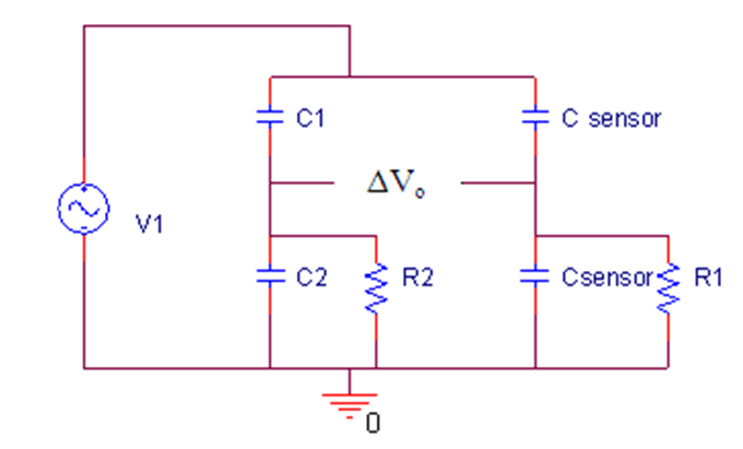
I want to amplify the output voltage of the bridge(ΔVo) in the circuit which is attached. The amount of capacitances are 47 nanofarad in balanced state & the power supply is a sine wave with frequency of 2.6MHz & amplitude of 0.8 volt. I used a xr2206 ic for producing the sine wave. R1 & R2 are 10k. Csensor is variable & its maximum is 85 nf. maximum ΔVo is 140mv & it's very low, so I want to amplify it, but the problem is that even AD829 ic can't amplify it. i don't know what the problem is . I will be gratful if anyone can help me. please tell me how i can amplify this voltage.
thanks.
 

You can increase input voltage.
Use instumentation amplifier.

22_1318841147.gif
[/url]

The two non-inverting amplifiers form a differential input stage acting as buffer amplifiers with a gain of 1 + 2R2/R1 for differential input signals and unity gain for common mode input signals. Since amplifiers A1 and A2 are closed loop negative feedback amplifiers, we can expect the voltage at Va to be equal to the input voltage V1. Likewise, the voltage at Vb to be equal to the value at V2.

As the op-amps take no current at their input terminals (virtual earth), the same current must flow through the three resistor network of R2, R1 and R2 connected across the op-amp outputs. This means then that the voltage on the upper end of R1 will be equal to V1 and the voltage at the lower end of R1 to be equal to V2. This produces a voltage drop across resistor R1 which is equal to the voltage difference between inputs V1 and V2, the differential input voltage, because the voltage at the summing junction of each amplifier, Va and Vb is equal to the voltage applied to its positive inputs.

However, if a common-mode voltage is applied to the amplifiers inputs, the voltages on each side of R1 will be equal, and no current will flow through this resistor. Since no current flows through R1 (nor, therefore, through both R2 resistors, amplifiers A1 and A2 will operate as unity-gain followers (buffers). Since the input voltage at the outputs of amplifiers A1 and A2 appears differentially across the three resistor network, the differential gain of the circuit can be varied by just changing the value of R1.

The voltage output from the differential op-amp A3 acting as a subtractor, is simply the difference between its two inputs (V2 - V1) and which is amplified by the gain of A3 which may be one, unity, (assuming that R3 = R4). Then we have a general expression for overall voltage gain of the instrumentation amplifier circuit as:

Instrumentation Amplifier Equation
98_1318841147.gif


As signal is ac and have no offset, use split supply to work in negative region or add an offset in positive region.
 
Status
Not open for further replies.

Part and Inventory Search

Welcome to EDABoard.com

Sponsor

Back
Top