Continue to Site

Welcome to EDAboard.com

Welcome to our site! EDAboard.com is an international Electronics Discussion Forum focused on EDA software, circuits, schematics, books, theory, papers, asic, pld, 8051, DSP, Network, RF, Analog Design, PCB, Service Manuals... and a whole lot more! To participate you need to register. Registration is free. Click here to register now.

Altium PCB designer - some component changed its layer color

Status
Not open for further replies.

loops0901

Newbie level 1
Joined
Apr 3, 2012
Messages
1
Helped
0
Reputation
0
Reaction score
0
Trophy points
1,281
Activity points
1,290
PCB designer.PNG
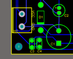
I am using altium designer to design my PCB board. Initially, all component layers are the yellow color. However, after i clicked for auto route, some components just changed to green color. I do not think components are overlaying the tracks. Does you guys have any ideas about this?

Beside, i send this PCB gerber files to my PCB supplier and they replied that the holes and pads does not match each others. The image below is the feedback from them.
issue.PNG

Please advice me about these issues. Thank you very much
 

The green color indicates design rule vialotaions. Place the mouse over the component and you can see the violation on headsup display menu.

The other issue, may be you used different origins while generating the gerbers. You have option for choosing relative and absolute origin while generating gerbers.
 

The drills have different offsets, so it's not a simple geber origin problem.

At first sight, I guess you have either combined files from different board versions or there's a problem in component definition. You should inspect the generated gerber and drill files thoroughly in Camtastic window.
 

FvM,yes you are right.Its not the problem with origin.
Loops0901, if possible post the pcb file so that we can have a look on it.
 

Status
Not open for further replies.

Part and Inventory Search

Welcome to EDABoard.com

Sponsor

Back
Top