Continue to Site

Welcome to EDAboard.com

Welcome to our site! EDAboard.com is an international Electronics Discussion Forum focused on EDA software, circuits, schematics, books, theory, papers, asic, pld, 8051, DSP, Network, RF, Analog Design, PCB, Service Manuals... and a whole lot more! To participate you need to register. Registration is free. Click here to register now.

Altium clearance of a polygon in bottom solder layer

Status
Not open for further replies.

azadfalah

Full Member level 2
Joined
Aug 13, 2016
Messages
145
Helped
1
Reputation
2
Reaction score
2
Trophy points
1,298
Activity points
2,423
HI everyone

I created a polygon in the bottom solder layer , but it does not observe any clearance

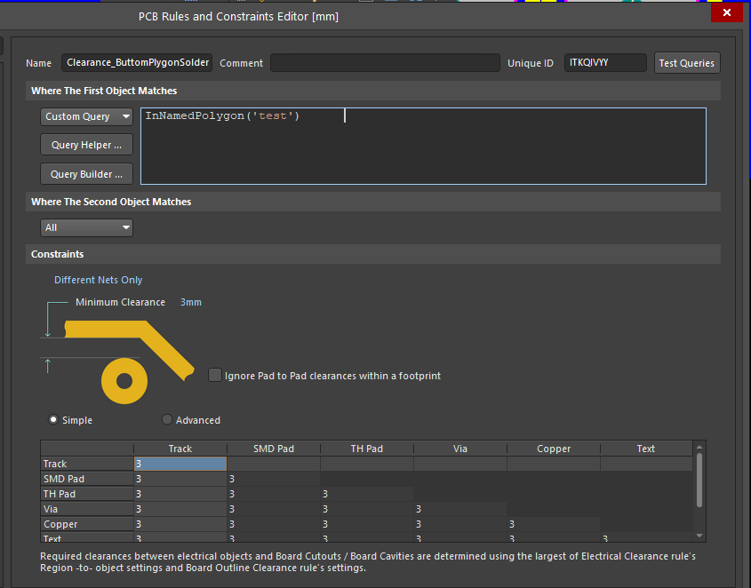
I even defined the rules specifically, but it does not work
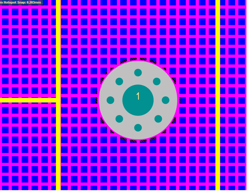
2.png


rules specifically
1.PNG


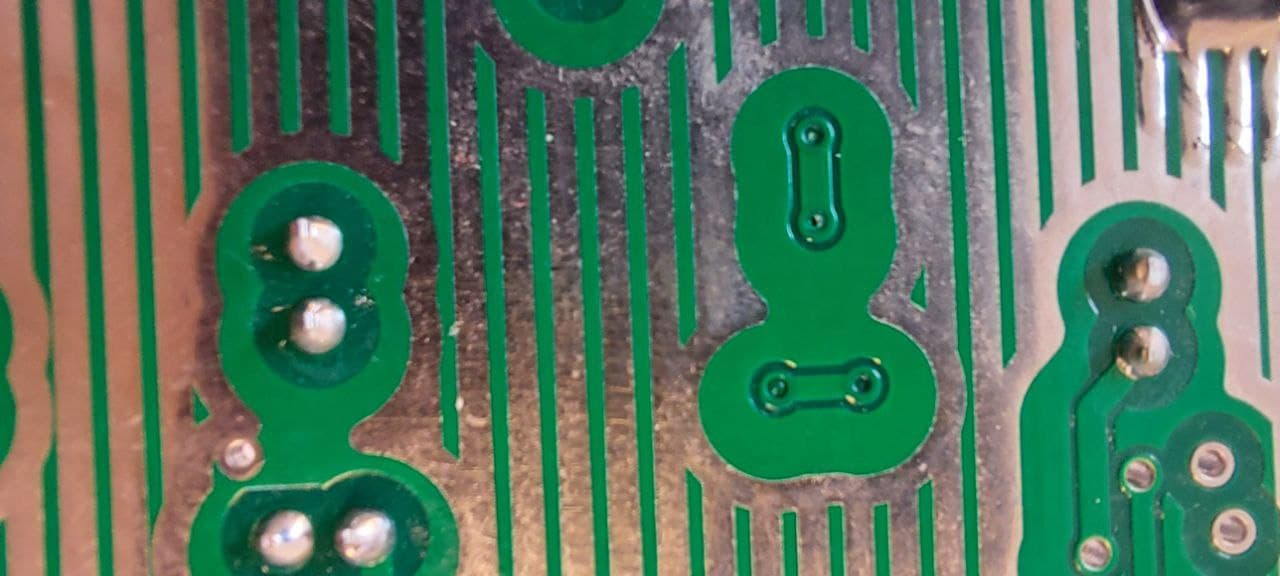
I want it to be like this
3.jpg


Thanks
 

You mean solder mask layer? Clearance to which objects?
Yes bottom solder mask layer, in older versions of Altium if you add polygon in solder mask layer the polygon draw with clearance from different net pads/via like last image but in newer versions it goes over the pads

Please guide me to have a polygon in the bottom solder mask layer as in the last image
 

Status
Not open for further replies.

Part and Inventory Search

Welcome to EDABoard.com

Sponsor

Back
Top