Continue to Site

Welcome to EDAboard.com

Welcome to our site! EDAboard.com is an international Electronics Discussion Forum focused on EDA software, circuits, schematics, books, theory, papers, asic, pld, 8051, DSP, Network, RF, Analog Design, PCB, Service Manuals... and a whole lot more! To participate you need to register. Registration is free. Click here to register now.

[SOLVED] Acitve loop filter for PLL

Status
Not open for further replies.
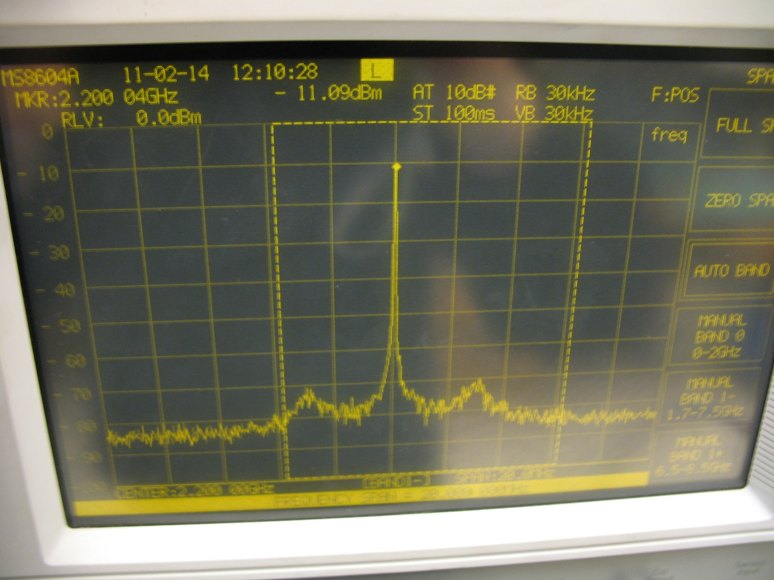
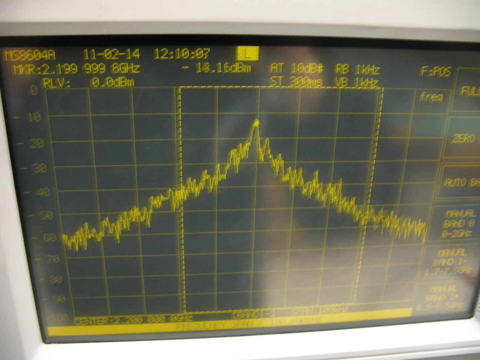
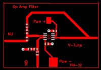
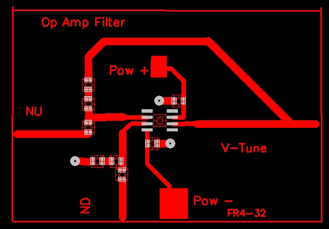
Hi again, I'm really stuck. Here is pcb of my filter. Can you see something wrong with it?


Three pads are ground vias. I'm using AD8675.

PLL is HMC698PL5.
 

Looks good to me. Not working? I do not see any resistor between vco tune line and op amp output, you could try that if it is either forward biasing the varactor at start-up, or if the vco has some hidden tune port capacitance that is driving the op amp nuts. 220 ohm should be enough.

The closed loop gain on the data sheet shows the bandwidth is limited to around 100 KHz at high gain, but that should not be a problem for your circuit. Never the less, try reducing your R and C values for 1/10th the open loop bandwidth just to see if it locks up normally.

Finally, are you sure you have the NU and ND pins right? Try reversing them just for yucks, and see if it locks up. The pll needs a negative feedback control loop, and sometimes one messes up and just hooks up the parts with the wrong polarity.

And you have good short connections between the phase detector and this board, and between this board and the VCO? Especially the ground connections? Also, make sure you do not have too long of a wire between this board and the power supply.

And are you sure you are programming the phase detector right? Some of them are hard to program (easy to get one bit set wrong) and then it does not lock up where you expect it to. Sometimes you can inject test signals into it and see if the divisors are set up like you expect them to be, or you might have access to test pins to check the divisor settings.
 

Hi, vfurlan,
Could you pls tell us your equation about N=PA+B?
What is your N, P, A, B respectively?
 

You can read ADF4106 for understand N, P, A, B, that's the reg setting for PLL chip.
 

I'm using HMC698LP5. If I understand correctly A = 6, B = 2, P ? (don't know). There is reference to P = 4, this should be minimum.

My is N = 22 for sure, I set it up correctly.
 

So N=22, I guess your setting is N=22=PB+A, so your P=4, B=5, A=2. This point could cause the problem, B should be greater than A. You must couble check your B and A, to ensure that B>A.

Other cause VCO bad PN as following:
1. The ref signal power level is too big.
2. OpAmp noise is too big.
3. PLL chip should have LDO for power supply.
4. VCO has bad performance.
5. Power supply of VCO has modulation signal.

PS.
just change the P A B equations.

---------- Post added 08-02-11 at 00:10 ---------- Previous post was 07-02-11 at 23:50 ----------

You can set N=44 , Freq Ref=125M to try to lock.

---------- Post added at 00:16 ---------- Previous post was at 00:10 ----------

And you should read out what is your N, Sel, and S value to post here.
 
Last edited:
I think you setup wrong value for the reg. You set N=22, so your prescalar is N*Sel+S, that is the problem.
 
Hello again,

i made progress, but I still need to do a final step.

200khz
50MHz
Setup

With AD8675, and some fine tuning I manage results you can see in the attached pictures. Now C = 10uF, R1 = 270Ohm, and R2 = 560Ohm. PLL is locked, and working fine.
As you can see, with 200kHz span, I still have some noise. What do you think, is this good enough, and if not what else can I do?

Thank you
 

It looks like you have a 2 MHz open loop bandwidth (from the 50 MHz plot). That plateau +/- 2 Mhz is the VCO locked to the crystal reference, with all the op amp and pll chip noise making a noise floor that is fairly flat. The noise peaks at 2 Mhz from the center tell me the loop is not as stable as it can be. Those peaks should only be a few dB at most above the flat part closer to the carrier.
 
This is what I have now. I'm concerned about noise. Is this good enough? I realy can get lower noise.


Well, at least you have it locked. Since you are a neophyte, before you go much further try doing a lot of tests on the PLL just as it is. What is the settling time? How much phase margin do you have? What is your control loop bandwidth? Do those parameters change as you vary the PLL chip divisor ratios? Does noise on the power supply rails lead to sideband noise at RF, and how many db down?
 
I succeeded in make this f*****g thing work. Thank you all.
 

Status
Not open for further replies.

Similar threads

Part and Inventory Search

Welcome to EDABoard.com

Sponsor

Back
Top