sys_eng
Full Member level 4


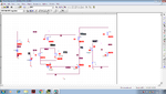
On the diagram, circuit on the right
1)how does Vi comes across into Ri?It's not obvious to me. iO is Vi / Ri. I see vFB across Ri but I don't see Vi across Ri.
Follow along with the video below to see how to install our site as a web app on your home screen.
Note: This feature may not be available in some browsers.

The circuit acts like a differential input operational amplifier and, with the negative feedback from the resistor to the negative input, strives to keep the voltage at its negative input equal to its positive input.
Any deviation of the minus input from the positive input will cause the output to change until the two voltages are again equal.
This means the voltage across R1 equals Vi.
Make sense?
If it's still not clear, try reading some tutorials on operational amplifiers.

1) If MT and M5 are the same size transistors then their ideal bias currents will be the same.1)the IBias on MT and M5 are not the same right?
2)if IBias on M5 increase VG would decrease and vice versa.
1) If MT and M5 are the same size transistors then their ideal bias currents will be the same.
2) No, VG would increase with an increase in IBias.
Try removing M5's drain from ground and connect it to M4's drain.
With floating Vout node, you'll hardly achieve any current through R1 or non-zero Vfb.
Even with M9 drain tied to Vdd, the circuit dimensioning is most likely unsuitable for M9 Id of 2 mA.

You're ignoring the simple fact that M9 needs a positive Vds for operation. There must be a load able to maintain the voltage under current. Connecting another high impedance node (the inverter input) can't solve the problem.

You obviously realized that M9 isn't able of sourcing 2 mA, thus you changed R1 to 10k. Unfortunately M9 can't even source 200 µA.still VFB doesn't track VI, VI=2V and VFB only 665.2mV
typo,Vgs(M4)=2-0.6026=1.3974V , Vgs(M5)=0.6652V and Ids(M5)>Ids(M4)..
How it's possible ??
You obviously realized that M9 isn't able of sourcing 2 mA, thus you changed R1 to 10k. Unfortunately M9 can't even source 200 µA.
Next step towards real CMOS design is to size transistors appropriately, e.g. give M9 a width multiplier of 16 or more.
You obviously realized that M9 isn't able of sourcing 2 mA, thus you changed R1 to 10k. Unfortunately M9 can't even source 200 µA.
Next step towards real CMOS design is to size transistors appropriately, e.g. give M9 a width multiplier of 16 or more.