Continue to Site

Welcome to EDAboard.com

Welcome to our site! EDAboard.com is an international Electronics Discussion Forum focused on EDA software, circuits, schematics, books, theory, papers, asic, pld, 8051, DSP, Network, RF, Analog Design, PCB, Service Manuals... and a whole lot more! To participate you need to register. Registration is free. Click here to register now.

About connection of the Filter and VCO in PLL design

Status
Not open for further replies.

gaom9

Full Member level 4
Joined
Oct 8, 2007
Messages
228
Helped
7
Reputation
14
Reaction score
5
Trophy points
1,298
Location
China
Activity points
3,294
vco connections

Hi,
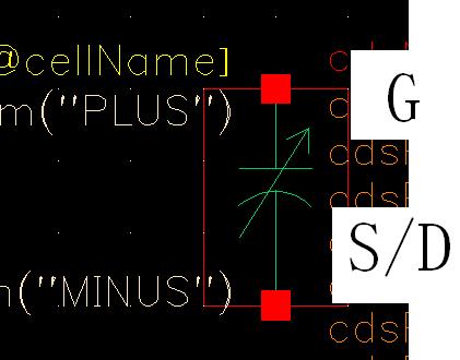
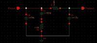
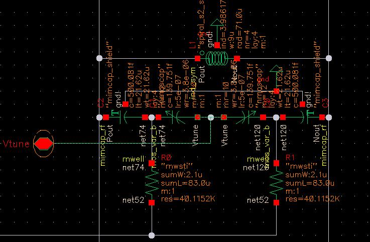
I am working in a Δ-Σ Fractional-N Frequency Synthesizers, I have a question about the connection of the filter and VCO in the circuit. The varactor of the VCO is AMOS as shown in Fig.1, the Vtune Voltage is directly connected to one port of the AMOS.


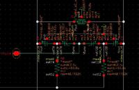
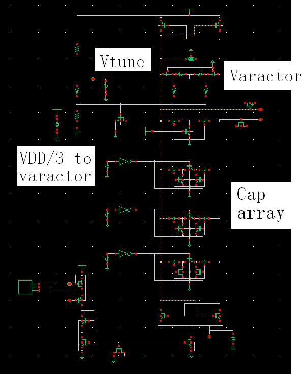
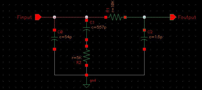
The loop filter is off-chip and 3order as shown in Fig.2.


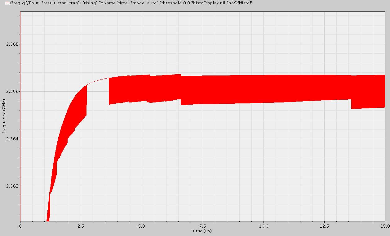
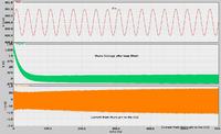
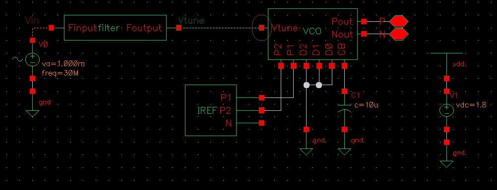
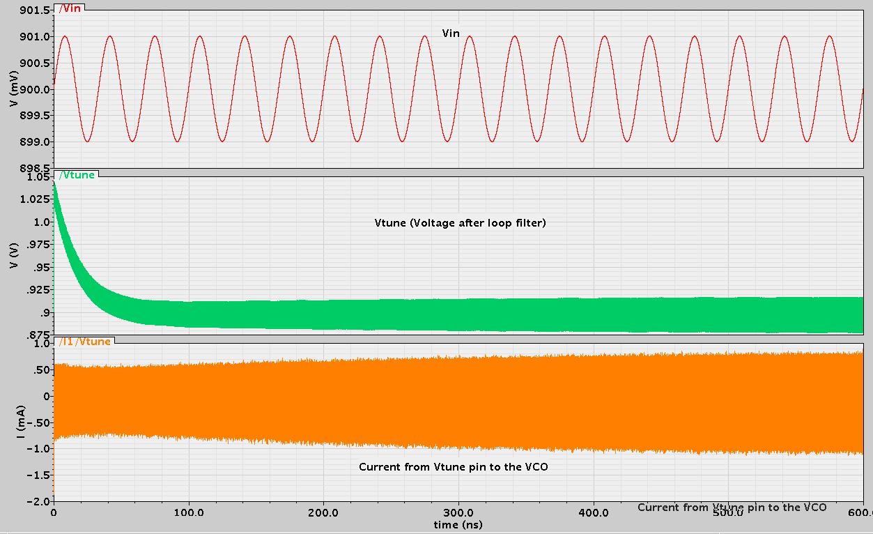
In the total circuit system connection, I connect the Filter and VCO directly, but, I found, the Vtune Voltage after the loop filter will be distorted, and a large current flow in to/out from the VCO, and this makes a large spurious tones to the Voltage signal, and makes it not stable. The voltage added to the filter (Vin), voltage after the filter (Vtune) and the current into the VCO are shown in Fig. 3


And I think I only need the Voltage value in VCO tune, the Current is unwanted, and I should removal the current, is that right?
I try to add a large resistor between the filter and the VCO to limit the current, and the VCO work well, but what I worry is that is the method right? what value the resistor shoule be and shoule it be off-chip? and is the resistor added here will effect the loop filter zero/pole? Or should I make any change in the VCO tune voltege input pin design, please?

Thank you!
Best regards!
 

site:www.edaboard.com gaom9

gaom9

it seems that, at 30MHz the impedance seen from the varactor pin is low (roughly 25 Ohm). It should be very high if the varactor is well biased.

From the external control you are biasing it a 0V (that shouldn't be the real situation, I guess, and I expect to see there VCC/2), but internally the bias is not shown.

Be sure that your varactor is reverse biased.

I hope it can help.

Mazz
 

    gaom9

    Points: 2
    Helpful Answer Positive Rating
preventing varactor diode forward bias vco

Thank you, Mazz!
The varactor is biasing to 1/3*Vdd. The DC biasing voltage is added from the 40K resistor in the two side of the varactor, should it right? Or should I change the biasing point.
In this AMOS, when biasing it to 1/3*Vdd the capacitor will be more linear in the whole range 0~1.8V.

Added after 9 minutes:

75_1236431866.jpg

The varactor is shown above. What type is reverse biased, what type is positive biased, please.

Thank you.
Best regards!
 

varactor symbol

Sorry, I made a mistake. You said MOS varactor but I was thinking to junction varactor, so I talked about forward/reverse polarization.

But now you show the gate in varactor symbol and you connected the S/D to Vcontrol. Try inverting varactors in VCO, so their gate will be connected toghether. Gate is isolated and you'll see an high impedance from that point.

I hope it can help.

Mazz
Mazz
 

    gaom9

    Points: 2
    Helpful Answer Positive Rating
psd pll

I have tried that method, but the input current will be more large....
The current is AC current, can it go thouth the MOS varactor?
I don't know why...
 

pll vtune offset

Yes, but it's not clear why you see a low impedance. Is it the Varactor VERY large?
Did you simulate the VCO?
You should try to simulate the VCO freq vs DC control voltage to see if it works properly.

Mazz
 

pll dither

Hi, Mazz
Thank you for your reply.
I have simulated the VCO freq vs the DC tune voltage, and it works well, the Kvco is about 50MHz/V, so I have to limite the output dither.

Best regards!
 

vco connection

gaom9 said:
75_1236431866.jpg

The varactor is shown above. What type is reverse biased, what type is positive biased, please.

Thank you.
Best regards!

Hello gaom9,
don't know what AMOS means. If it's an NMOS, the Gate should be the positive terminal, for a PMOS, the G terminal should be the negative one (against S/D=VDD or below).

For my process (std. CMOS 0.18µ), the strongest C vs. V dependency is around 0V for (Vg-Vsd), not around 1/3*VDD, in the voltage areal (Vsd ± Vth).
 
vco vtune circuit

Hi, erikl
AMOS is a type of MOS, it is a NMOS on NWELL. It is with a good capacitor linear than general MOS. My process is TSMC 0.18, For the charge output voltage range need, I should bias the AMOS to 1/3*VDD to get a linear in 0.4-1.4V. The C vs V dependency is not around 0 in this capacitor something not the same as NMOS and PMOS.
And I have tried the differenct connection of the S/D and G terminal, but the current is still.

Thank you.
Best regards!

Added after 3 hours 34 minutes:

Hi
I am sorry I made a mistake, when I add a large resistor between the filter and the VCO input, the current unwanted can be limited, but the VCO tune Voltage is still have a large dither. Adding a large resistor can not solve this question.
And I add a large capacitor to ground at the connect line between filter and VCO, the AC current will be filter out, but the bandwidth will be change...
So, is there any mistake in my filter design? But I find this type of filter is used in many papers.
 

using high vtune vco in pll design

gaom9

Do you know that the filter is current driven by a charge pump and not by a voltage source?

Mazz
 

Hi, Mazz
I know the filter is driven by the charge pump current. But my question is that when I use the 3rd order filter, the voltage in the two edge of R1 is not the same, and the voltage of the charge pump output is with much less dither than the voltage at the tune voltage node of the VCO.
Yestoday, I try to used the 2nd order filter, and because there is not resistor between the output node of charge pump and the input node of VCO, the voltage can keep the same. But when the tune voltage keep stable, the VCO output is with large dither, either. I think the input current of the VCO result in this dither, this current go through the DC biasing resistor and change the DC bias point of the varactor.
How to reduce this effect?

When I used the PSS simulation to analyse the VCO alone, the VCO can work well with a certian DC tune input.

And how to make sure the Voltage added between the varactor keep stable when the Vtune voltage is stable so the keep the capactor of varactor the same and a DC biasing is added to one node of the varactor, please?

I tried to used three 3MΩ resistors to generator Vdd/3 dc biasing voltage, and for the so large resistors, the DC bias can keep stable, and the output is with less dither, but the resistors are too large....
How can I generator a Vdd/3 DC voltage, please?

Thank you!
Best regards
 

Gaom9

is not really clear what you intend with "dither". Could you please explain?
When PLL is in lock state, the charge pump injects some small pulses into VCO control, but the mean voltage is stable.
In integer N PLL this is at reference freq, that has to be filtered out by loop filter, and, as it isn't ideal filtering, some signal is injected and this appears as a spur.
The only problem that I see in your circuit (and I'm not able to explain it) is that the VCO control seems to be a low impedance.
BR
Mazz
 

Hi, Mazz
Thank you for your reply.
The dither of the output signal frequency here means when the tune voltage of VCO become stable but the output frequency is still changing. I think it is because of the current flows into the VCO tune voltage port and flows the DC biasing resistor so to change the voltage between the Varactor.
I agree with you, that the VCO control seems to be a low impedance. But I tried PMOS and AMOS as varactor, the current is still.
How to increase the impedance of the VCO control? and what value of the current should I limit to? How to generate a DC biasing voltage with a high impedance, please?

Thank you!
Best regards!

Added after 1 hours 35 minutes:

Hi, Mazz
I think the connection of the Varactor in VCO is as the same with others. But the current unwanted is still very large. Is it something matter with the spice Model?
I use the TSMC 0.18um PDK to simulate the VCO.
 

Are you sure that the VCO is completely balanced?
 

Hi, saro_k_82
I think my VCO is balanced. It can pass the PSS analyse in spectre with a DC tune voltage input.
But when I use the freq function in cadence to calculate the frequency of the output signal vs time, the frequency value is not stable, and it is with a large dither.
Besides the PSS analyse, what simulation should be done to make sure it is completely balanced?

Thank you.
Best regards!

Added after 25 minutes:

The tran simulation result is shows in the following figure.
Output frequency vs Time of the VCO


The circuit diagram of the VCO is as following


Imbalance will not prevent PSS from converging. Imbalance between the two output nodes can easily cause currents at the VTune node. When one node rises by dV, if the other node goes down exactly by dV, the currents through the cap will be of same magnitude and there will be no residual current at the VTune node. Just check whether both the signals are exactly off by 180 deg.
 

Hi, saro_k_82
Thank you for your advice.
I find the waveforms at the two nodes have some difference, so I change the circuit parameters, and make sure the two waveforms exactly off by 180 deg and have the same shape. The current flows into the filter becomes much smaller which is about 40nA.
But I use the "freq" function to calculate the frequency value of the output signal, it still have a about 500KHz dither when the input a DC voltage into the filter, is it too large?

And another question, for example, when I use the PSS analyse, the output frequency value is 2.440GHz, but I use the "freq" function to calculate the frequency, the frequency is 2.388GHz, which should I trust? Because I need to confirm the frequency tuning range of the VCO.

Thank you!
Best regards!
 

PSS is the one you should be trusting. Transient sims are used to quickly estimate the frequency and not expected to provide accurate results about the frequency domain. Tran is prone to lot of numerical errors (a very small error at the threshold can show up as an observable frequency noise).
500K is too small on a 2.4G scale., don't worry about this. Just run the same tran with tighter tolerances and errpreset=conservative and you'll see it reducing.
Plot the PSS frequency spectrum and see whether you see any tones at 500K, if it is not present, then it was artificially generated by tran sim.
Run a pnoise analysis along with the PSS to get the exact phase noise of the VCO., this is what you need to be worried about., If this looks ugly., we'll look where to attack., otherwise there is no problem with your circuit.
 

    gaom9

    Points: 2
    Helpful Answer Positive Rating


Hi, saro_k_82

The PSS frequency spectrum and Phase noise figure is shown above.
There is no tones at 500K, so it was generated by tran sim.
And the phase noise is -124.5dBc/Hz at 1MHz offset, I think it is enough for my use.

My problem has been solved.

Thank you, everyone.
Best regards!
 

The fact that PSS does not show a tone at 500K does not mean that it is clean there. The PSS fund that you have set is 2.4GHz, and so it operates over a time period of 417p. To show what is happening at 500K, it has to operate over 2us. If you provide an estimate 0f 500K for the PSS sim, the PSS might still converge for 2.4GHz as the 500K component can be very small. So you need to run a transient with tight tolerances, take the dft and observe the 500K component
 

Status
Not open for further replies.

Part and Inventory Search

Welcome to EDABoard.com

Sponsor

Back
Top