Continue to Site

Welcome to EDAboard.com

Welcome to our site! EDAboard.com is an international Electronics Discussion Forum focused on EDA software, circuits, schematics, books, theory, papers, asic, pld, 8051, DSP, Network, RF, Analog Design, PCB, Service Manuals... and a whole lot more! To participate you need to register. Registration is free. Click here to register now.

a low gain stage implementation with mosfets

Status
Not open for further replies.

perado

Full Member level 2
Joined
May 28, 2010
Messages
127
Helped
2
Reputation
4
Reaction score
2
Trophy points
1,298
Activity points
2,134
Hi
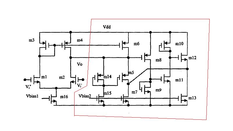
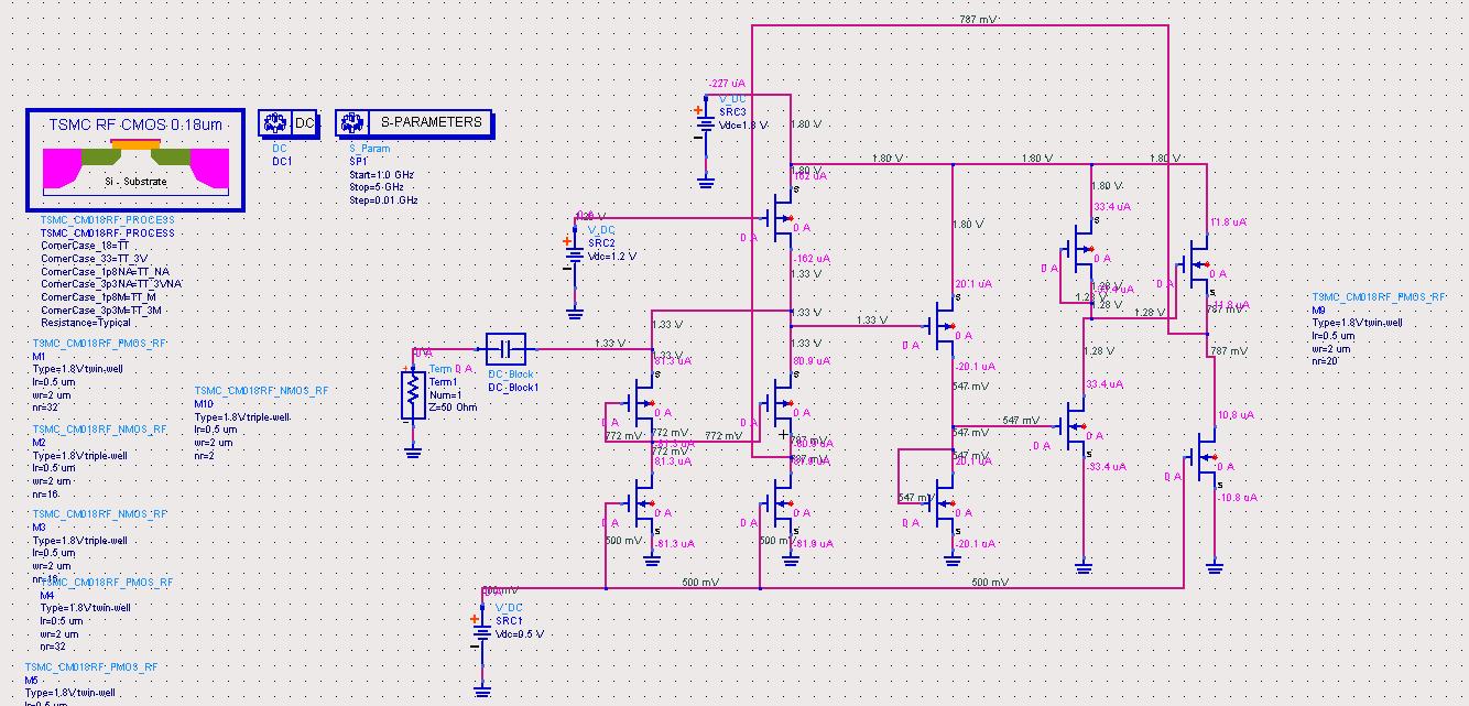
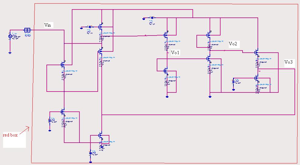
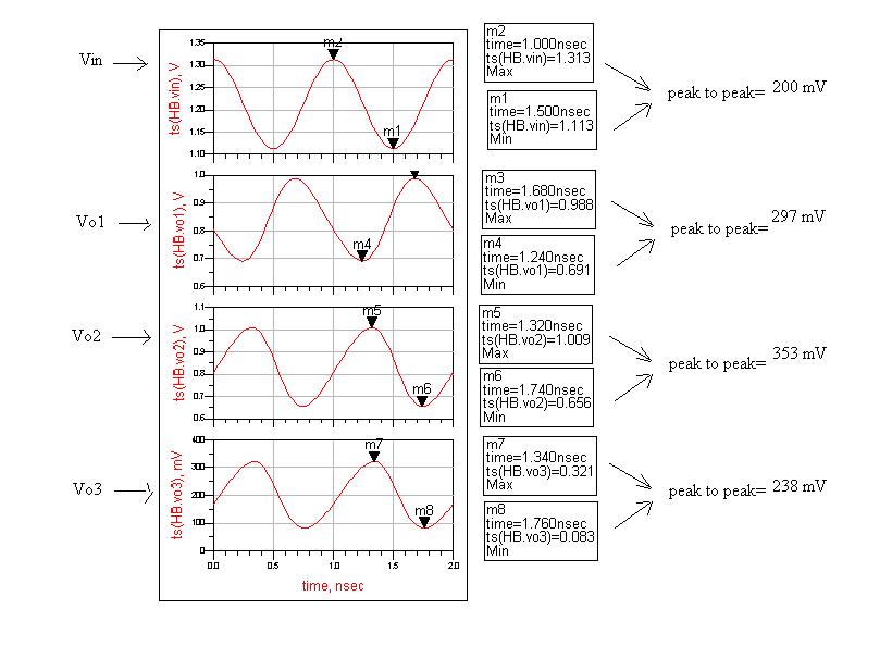
I want to simulate this circuit schematic:

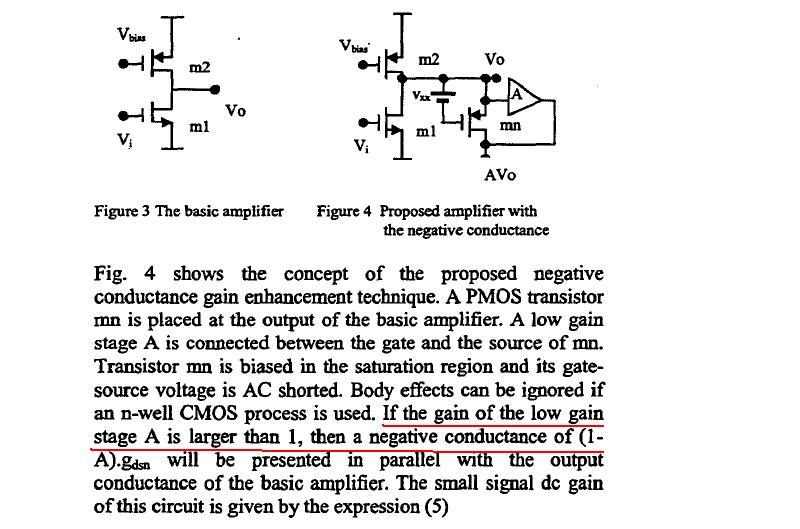
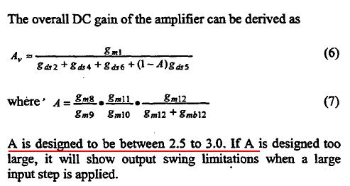
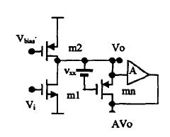
A is a low gain stage, but I dont know how can I implement it with mosfets, can anyone show me a circuit diagram that can replace as A
 

I thought you can use CS amplifer , becuase the Block has hanged in parallel with the MOS in the sense it should bot disturb the Vo , so it should have high input impedance.
 

Where does this node 8475689700_1455701044_thumb.jpg go to? Is it a resistor or a current sink to GND ?
 

Where does this node View attachment 126197 go to? Is it a resistor or a current sink to GND ?
I think a current sink
it is based on this paper:
**broken link removed**
the final proposed circuit of this paper is:

it seems that the red box circuit should act as negative conductance, but my simulation result for Z(1,1) is not negative
 
Last edited:

A current sink, right (m7).

So m8 .. m13 obviously is the low gain stage A. I'd think it depends on its gain if the circuit acts as negative conductance.
 
  • Like
Reactions: perado

    perado

    Points: 2
    Helpful Answer Positive Rating
A current sink, right (m7).

So m8 .. m13 obviously is the low gain stage A. I'd think it depends on its gain if the circuit acts as negative conductance.
all the transistors should be in saturation, is it true?
Do you have any idea help me to do correct simulation?

 
Last edited:

all the transistors should be in saturation, is it true?
Sure.

Do you have any idea help me to do correct simulation?
Sorry, I neither have the time nor your simulator & simulation models. Just can give you some advice. First isolate A (m8 .. m13) and try and get its gain a little bit >1 : if it's too much over 1, it will oscillate.
Play with the W/L ratios of the transistors. Then reconnect it and simulate the whole amp.

4 notes:
1. You didn't connect the transistor substrates. Is this done automatically by your tool?
2. You can never expect to measure a negative conductance at Vo - and you ruin the amp's gain as long as you have a 50Ω load connected to it.

The aim of this amplifier is to achieve a huge output resistance (at node Vo) with the help of this negative conductance circuit part (the red box above).

Means:
3. you can only achieve and measure a negative conductance at the red box part - not at the whole amplifier.
4. you must not load the output Vo at all - this is the precondition to achieve high gain with a single stage amp.
 
  • Like
Reactions: perado

    perado

    Points: 2
    Helpful Answer Positive Rating
Sure.


Sorry, I neither have the time nor your simulator & simulation models. Just can give you some advice. First isolate A (m8 .. m13) and try and get its gain a little bit >1 : if it's too much over 1, it will oscillate.
Play with the W/L ratios of the transistors. Then reconnect it and simulate the whole amp.

4 notes:
1. You didn't connect the transistor substrates. Is this done automatically by your tool?
2. You can never expect to measure a negative conductance at Vo - and you ruin the amp's gain as long as you have a 50Ω load connected to it.

The aim of this amplifier is to achieve a huge output resistance (at node Vo) with the help of this negative conductance circuit part (the red box above).

Means:
3. you can only achieve and measure a negative conductance at the red box part - not at the whole amplifier.
4. you must not load the output Vo at all - this is the precondition to achieve high gain with a single stage amp.

Hi
thanks for your advices, I try to use them and I hope leads to desired results,
some notes:
1-I dont want to simulate whole amp and just I want to simulate and show the negative conductance of red box, and then use it for other circuits.
2-you are right, I should correct my schematic for simulation, and connect pmos body to VDD and nmos body to GND
3-in the picture of my simulation setup that I had attached, I draw just the red box part and I did not want to load it with 50ohm , but I put a term 50ohm and a dc block just for simulation and measure the input resistance of the red box part, before this I did a simple simulation in my simulator like this picture:

it seems that 50ohm term dont load the desired circuit, and after simulation Z(1,1) and Y(1,1) are input resistance and conductance of two 400ohm resistors without 50ohm term

- - - Updated - - -

it is my final simulation setup and the waveforms of nodes that showed in picture, ofcourse it dont get me negative conductance yet:thumbsdown:


it seems that 50ohm term dont load the desired circuit, and after simulation Z(1,1) and Y(1,1) are input resistance and conductance of two 400ohm resistors without 50ohm term
Good! It seems your terminator is just a virtual 50Ω resistance, not a real one. So what is it for?

it is my final simulation setup and the waveforms of nodes that showed in picture, ofcourse it dont get me negative conductance yet :thumbsdown:
Did you trim the circuit for a gain of a little bit more than 1 ?

BTW: You can measure its conductance only at node Vin.
 

Good! It seems your terminator is just a virtual 50Ω resistance, not a real one. So what is it for?


Did you trim the circuit for a gain of a little bit more than 1 ?

BTW: You can measure its conductance only at node Vin.
I dont know what is it for, but it is the proposed technique (simulation setup) for measure the input impedance of a circuit by the ADS simulator, and should be placed a 50ohm term at the node that we want to measure input impedance
Yes, I try to design the circuit for a gain little more than 1, ofcourse the waveforms that I had attached showed the Vin is 200mV peak to peak and Vo3 is 238mV, before common drain stage I achieve more gain (near 2 or 2.5) , can I delete the common drain stage or it is needed??
Yes, I had measured the conductance at Vin, and 50ohm term connected to this node
 

I dont know what is it for, but it is the proposed technique (simulation setup) for measure the input impedance of a circuit by the ADS simulator, and should be placed a 50ohm term at the node that we want to measure input impedance
Ok, probably an ADS specialty (I don't know this simulator).

Yes, I try to design the circuit for a gain little more than 1, ofcourse the waveforms that I had attached showed the Vin is 200mV peak to peak and Vo3 is 238mV,
May be this gain is too high. Try to get it to 1.0 ≤ gain ≤ 1.05 .

before common drain stage I achieve more gain (near 2 or 2.5) , can I delete the common drain stage or it is needed??
Yes, the source follower is needed for low output impedance, because it doesn't connect to a gate, but to a node with lower impedance.

Yes, I had measured the conductance at Vin, and 50ohm term connected to this node
Ok. May be you cannot measure a negative conductance directly. Test the conductance difference of the single stage amplifier without and with the red box circuit. It should be lower (impedance higher) when the negative conductance circuit (NCC) is connected to it (Vin to Vo).

Take care that you don't change the DC node voltage by the connection, because neither the DC output impedance of the one-stage-OTA nor the Vin impedance of the red box (NCC) is infinite. That means Vo and Vin should be the same before and after the connection.
 

Ok, probably an ADS specialty (I don't know this simulator).

May be this gain is too high. Try to get it to 1.0 ≤ gain ≤ 1.05 .


Yes, the source follower is needed for low output impedance, because it doesn't connect to a gate, but to a node with lower impedance.


Ok. May be you cannot measure a negative conductance directly. Test the conductance difference of the single stage amplifier without and with the red box circuit. It should be lower (impedance higher) when the negative conductance circuit (NCC) is connected to it (Vin to Vo).

Take care that you don't change the DC node voltage by the connection, because neither the DC output impedance of the one-stage-OTA nor the Vin impedance of the red box (NCC) is infinite. That means Vo and Vin should be the same before and after the connection.
Hi dear erikl
the paper said about the gain (A) :

and it seems that the gain is not too high (maybe was low beacuse is less than 2.5)
I try to do your advices, and then show the results
 

Status
Not open for further replies.

Part and Inventory Search

Welcome to EDABoard.com

Sponsor

Back
Top