Continue to Site

Welcome to EDAboard.com

Welcome to our site! EDAboard.com is an international Electronics Discussion Forum focused on EDA software, circuits, schematics, books, theory, papers, asic, pld, 8051, DSP, Network, RF, Analog Design, PCB, Service Manuals... and a whole lot more! To participate you need to register. Registration is free. Click here to register now.

800MHz Power Amplifier Design Process

Status
Not open for further replies.

Mahruz

Junior Member level 3
Joined
May 16, 2022
Messages
28
Helped
0
Reputation
0
Reaction score
0
Trophy points
1
Activity points
335
Hi All,

I am kind of new to RF power amplifier design and I wanted to try and design a 800MHz RF power amplifier by myself using Microwave Office AWR .
I am trying to understand the design process involved in designing this 800MHz Power Amplifier.
From online books and videos, I understand the process to be as follows:
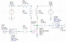
1. Obtain the transistor model. I am using NXP ( https://www.nxp.com/products/radio-...ideband-rf-power-ldmos-transistor:AFT09MS015N )
2. Chose a bias point. I wanted the PA to be a class A amplifier.
3. Perform stability analysis. Improve stability if rollet's factor is less than 1.
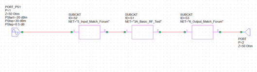
4. Design input and output matching networks against 50 Ohms.
5. Start with layout.( I have not reached layout part).
My questions are:
> Is the above process the correct process or did I miss out on any steps that can cause the PA not to function?
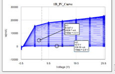
> How can I plot the loadline in AWR?
> Is there any example in AWR that a beginner can use to understand and replicate for a PA design?

Thank you for sharing your knowledge.
 

The process is partially correct. But No.4 is not true.
Power Transistors have Optimum Load Impedances that maximize either Delivered Power or PAE or Power Gain.
These three specifications cannot be maintained simultaneously and those Optimum Impedances are either given by manufacturer's Measurements ( Page 7 in Datasheet) or Simulated with accurate models. Measurements are generally correct.
These Impedances ( Source and Load ) must be matched to 50 Ohm, not Output/Input Impedances of the Transistor.

Layout is another story.

Look at also Ampleon that still manufactures a wide range of RF Power Transitors ( former NXP components )
There are many application notes and reference designs on their website. You can find easily an appropriate one.
--- Updated ---

Also look at
www.wolfspeed.com
 
Last edited:

Hi Big Boss,

Thank you for sharing and confirming the process.
In continuation to the 800MHz PA design; I have some more questions as below.
1. By using AWR to plot transfer character; I am confused to as where I should consider the saturation point starting from? Does marker 1 be considered as a good pointView attachment 178130
View attachment 178131


2. I plotted the IV using the below schematic and got the IV curve with further image.
Since I want a class A operation bias point for the PA; where should the Marker be located at?
Also, from the datasheet(https://www.nxp.com/docs/en/data-sheet/AFT09MS015N.pdf) ; I wanted to use the Table 8 specification which is VDD 12.5DC; IDQ = 100mA. But how do I obtain that plot/marker in AWR? Marker 2 is the closest I can get to 100mA. How can i get 100mA exactly?
1661249397949.png

1661249661037.png


3. The next step I did was stability circles.
The first image is without any series stabilization resistor adn the second image is the stability circle for the first circuit
1661249926942.png


1661249990678.png


I was able to stabilize the circuit by adding a series resistor to the transistor. But when I do so, the stabilization is good but the S21 drops from apprx 19dB(along with matching network) to 13dB. Is there a way to increase it? Like a different stabilization techniques?

4. Then I did input matching. The circuit is below. After designing the input matching network, the smith chart was close to 50Ohms at870MHz. I have not matching the output as of now. But the question is, from datasheet figure 8; where do I use the zsource/load information?
1661250196515.png

1661250224988.png


5. Similarly, I did from output matching as well and got the smith cart to 50 Ohms at 870MHz.
6. The final s values are shown in the below image. the schematics is following it. The question is, is this a good amount of gain and good loss?
1661250507098.png

1661250549060.png


Thanks all for advising me.
 

Attachments

  • 1661249588087.png
    1661249588087.png
    38.5 KB · Views: 116

The best is to use in your simulation input and output LTUNERs. And when the tuning is done, replace the tuners with LC components (a simple low-pass LC matching network should work).
I found on the net this basic example of a 30W 450MHz LDMOS power amplifier.
The transistor MRF9030 works up to 1GHz so you can try using it at 800MHz.
To verify further the linearity of the PA (for class-A) may need to run a two-tone test and check the IMD (have to add at the input, via a combiner, two RF power sources, about 100kHz spacing). As is mentioned in the MRF9030 datasheet.
 

Attachments

  • 30W_450MHz_MRF9030.jpg
    30W_450MHz_MRF9030.jpg
    307.3 KB · Views: 141
LTUNER is not necessary to analyze a simple IV Curves. BIASTEE component is sufficient.
1661285671300.png

Then you should squeeze the VGS voltage to obtain the right value.
1661285459264.png

The first step to verify the fundamental parameters by drawing a test set-up. You can enter Optimum Load and Source Impedances directly into Port elements
1661285687630.png

1661285962044.png

1661285982838.png

1661285998297.png


There are possibilities of discrepancy between measured data and model data. It's normal.
Now compare these results with datasheets' measured data.
I attach the project archive file you to inspire.
 

Attachments

  • ATF09MS015NT1_Test.rar
    2.6 MB · Views: 139
LTUNER is not necessary to analyze a simple IV Curves. BIASTEE component is sufficient.
View attachment 178152
Then you should squeeze the VGS voltage to obtain the right value.
View attachment 178148
The first step to verify the fundamental parameters by drawing a test set-up. You can enter Optimum Load and Source Impedances directly into Port elements
View attachment 178153
View attachment 178154
View attachment 178155
View attachment 178156


There are possibilities of discrepancy between measured data and model data. It's normal.
Now compare these results with datasheets' measured data.
I attach the project archive file you to inspire.
Hi Big Boss,

Thank you for sharing the AWR file. It was extremely helpful for a starter like myself.
I continued with the design and and had some more questions as below.


1. I plotted the Mu factor. My question is,
1.1] Do I plot the mu factor with only the bias network and no matching network?
1.2] My factor was above 1 from 760 to 870 MHz similar to that of the datasheet's design. But I wanted the mu factor to be above 1 from 500MHz to nearly 1GHz. So I added a series resistor. By doing so; the mu factor was above 1(not shown below) but when I plotted the input v output power graph, I got extremely low output power. So, how can I stabilize the FET beyond frequency of operation and still obtain good inputVouput power?
1661498425911.png


2.
I design an input matching network as shown below with the smith chart results. Port 2 is the Z source from the datasheet. From the smith chart, the matching looks good; is this correct?
1661497134877.png

1661497168451.png


3.
Similarly; I designed the output matching as well and the smith chart results. Again; I believe this is a good matching, right?
1661497305879.png

1661497332266.png


4. From my understanding; now, since, the input and output have been matched to 50 ohms with their respective source and load impedance from the datasheet.
So, I plotted the input power v output power graph again as shown below for the below circuit (the impedance is also written for clarification).
From the design file Big boss provided; I required 17.35dBm input to get 6W output. This was withOUT any input/output matching. And this was good. However, after performing the matching; the input requirement is now 26.76 dBm for 6W output. This increase in input power requirement, is it normal because of matching losses or did I do something wrong?

1661497625827.png

No matching
1661497875808.png

below is with matching

1661498054190.png


5. What are the next steps to be followed for me to continue the design? I know the layout comes next; but is there something else that I should take care of before moving to layout?

I have attached my AWR file; just in case you wanted to have a look at it. Unfortunately, it is not very pretty and clean!!

Thanks for your advise,
 

Attachments

  • 1661497512674.png
    1661497512674.png
    17.1 KB · Views: 124
  • 1.AFT09MS015N--Design - Forum.rar
    61.8 KB · Views: 109

First observation.
The Port Impedances must be complex conjugate of the Optimum Load/Source Impedances. If the transistor wants to see an impedance at both Input and Output, the Source Impedance(s) must have complex conjugate with Matching Circuit. Like that;
1661501608166.png

If you design the matching circuit carefully, you can obtain good results.
1661501723223.png

1661501752584.png

Consider Microstip Lines instead Inductances for Matching Circuits because low valued Inductances have bad tolerances.
View attachment 1661502486537.png
1661502349464.png
 

Hi Big Boss,

Thank you for sharing about the input/matching network.
That was the main cause for why I did not get good results.

>> I improved the input and output matching and was able to obtain 6Ws at 18dBm input, which is similar to its datasheet.
1661835878651.png


>> I was wondering if you can share some insights to the stability question in the previous thread. I am still a confused in this aspect.

>>Regarding S parameter plots; I get the below results. The S21 seems to be great; but the S11 and S22 is not that great. Any idea why this might be the case even though I get 6W at 18dBm input(same as datasheet) and the input/output is matched .
1661836952117.png


>> Lastly, moving forward, I was wondering; what shall be the next steps other than converting the input/output network to microstrips.

Thanks for your advise.
Mahruz
 
Last edited:

Don't worry about S11 and S22 because you have done Power Matching not Conjugate Matching.
This is normal for Power Amplifier because Small Signal Input and Output Impedances are completely different than Large Signal Optimum Load and Source Impedances.
In order to see where the "conditional instability" comes from, you check both Input and Output Stability Circles and then you place parallel resistance to push out the problem circle(s).
Don't insert series resistance because Impedances are very low and the amplifier will fall.
 
Hi All,
In continuation to above thread; I designed the matching networks for 870Mhz and it is very good.
However, I wanted almost similar output(above 6W) from 849Mhz to 870MHz.
So, I redesigned the matching to 860Mhz as it is the central frequency for the band I am looking for.
But as you can see, in the image below, after the mactching is done; at 849 and 870Mhz; there is very low power.
How can I make the design work for 849 to 870 MHz with at least 6W for the full band?


1662585366620.png


Thanks for your advise.
Mahruz
 

Seeing the high peak at center, it seems you have high Q (goes hand-in-hand with high selectivity).

Q is influenced by L:C ratio. Try reducing this by reducing L values and raising C values, a little bit at a time.
 
Seeing the high peak at center, it seems you have high Q (goes hand-in-hand with high selectivity).

Q is influenced by L:C ratio. Try reducing this by reducing L values and raising C values, a little bit at a time.
Hi BradtheRad,
Thanks for sharing that. I was able to change it and it was successful.
--- Updated ---

Hi All,
I was trying to convert the input matching network from lumped element as shown below(first image) to microstrip(third Image) with same performance(second image) but not sure on how to do so in AWR.
Not sure if I should use TLIN or MLIN or something else?
Please help.

1662973673814.png

1662973642508.png


1662973729198.png


Thanks,
Mahruz
 

Status
Not open for further replies.

Part and Inventory Search

Welcome to EDABoard.com

Sponsor

Back
Top