Continue to Site

Welcome to EDAboard.com

Welcome to our site! EDAboard.com is an international Electronics Discussion Forum focused on EDA software, circuits, schematics, books, theory, papers, asic, pld, 8051, DSP, Network, RF, Analog Design, PCB, Service Manuals... and a whole lot more! To participate you need to register. Registration is free. Click here to register now.

[General] 7 segment issue, dp doesn't work on 12v

Status
Not open for further replies.

sushant_21

Junior Member level 3
Joined
Apr 30, 2017
Messages
28
Helped
0
Reputation
0
Reaction score
0
Trophy points
1
Location
Mumbai
Activity points
269
(Help)

I am having problem in seven segment, the problem is when a-g segment glow, the dp is not glowing . DP only glow when rest of segments are off.

I have tried almost all that I can do from firmware,

I tried setting output port setting to open drain , disabling internal pull up. But it doesn't seem to work.

This is small code to lit every segment of 7seg every 1s.

Hers the video link for problem,

video

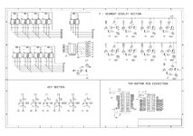
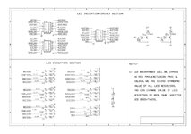
JP2 and JP3 IO lines are directly connected to LPC1768 IO pins.

I tried Removing R30 and placing 10k between Collector and DP.

Also tried changing R28 to 1.2k and removing r29

I have also tried Q11 transistor replacing with BC847, BC858 but its not working..

So finally I ask for your help, i believe it's hardware related , sadly hardware is developed by different party.

The problem is, I have always used 3.3V to drive segments, but here they used 12V , DP or led should work with 2n2222 but it's not couldn't get why
 

Attachments

  • CKT_DIA_CH5_PRO_TOP-V1.1_wo_name_page-0001.jpg
    CKT_DIA_CH5_PRO_TOP-V1.1_wo_name_page-0001.jpg
    897.9 KB · Views: 133
  • CKT_DIA_CH5_PRO_TOP-V1.1_wo_name_page-0002.jpg
    CKT_DIA_CH5_PRO_TOP-V1.1_wo_name_page-0002.jpg
    782.4 KB · Views: 132
Last edited by a moderator:

This is your LED 7 Segment part ?

1642067082712.png


If so not sure why the DP is driven differently than other segments. This is common anode.

Do you have the code for driving the display ?


Regards, Dana.
 

Hi,

the problem is that you wired the DP differently than all the other segments.
DP has no individual series resistor. While segments A...G have 150 Ohms resisitors (R21... R27)

Add a series resitor for DP.
Also you need to omit the digit_global resistors R39..R47.
Re calculate the resitor value for the segments.

Klaus
i have added a 1.2K resistor at DP but there is no change. i had done this earlier also, i had tried 470ohm, 1.2k or 3.3k resistor.

the global resistor R39 - R47 are to control brightness of 7seg, theres possibility that row1 is red and row2 is green 7segment, so both will have different resistor.
 

i have added a 1.2K resistor at DP but there is no change. i had done this earlier also, i had tried 470ohm, 1.2k or 3.3k resistor.
You need to do all the changes, not only one.


the global resistor R39 - R47 are to control brightness of 7seg, theres possibility that row1 is red and row2 is green 7segment, so both will have different resistor.
Does not work properly, because you don't know whether 2 segments (for a "1") is ON or 7 segments (for an "8")

Klaus
 

This is your LED 7 Segment part ?

View attachment 173847

If so not sure why the DP is driven differently than other segments. This is common anode.

Do you have the code for driving the display ?


Regards, Dana.
hi Dana thanks for reply, here id the code

C:
//                                d1, d2, d3, d4, d5,d6, d7, d8,    d9
const uint32_t DispLookup[] = {18, 19, 20, 21, 22, 23, 24, 25 ,26};
#define DISP_SEL_ENABLE 1

#define DISP_SEL_DISABLE 0

#define DISP_PORT 2

#define CS_PORT 1


void display_test()
{
    if(seg_counter > 7){
        seg_counter = 0; // reset segment_index counter

#if (CHANNEL_COUNT == 5)
        // clear all DS selection
        Chip_GPIO_SetPortOutLow(LPC_GPIO, CS_PORT, 0x7FC0000);
        
#else
        Chip_GPIO_SetPinState(LPC_GPIO, CS_PORT, DispLookup[seg_count], DISP_SEL_DISABLE); // disable first
#endif
        // increment DS x-counter
        seg_count++;
        //set DS of any DSx (select any1 ds)
        Chip_GPIO_SetPinState(LPC_GPIO, CS_PORT, DispLookup[seg_count], DISP_SEL_ENABLE);    // enable nxt

        if(seg_count > DISP_SEG_COUNT)
        {
            seg_count = 0; // reset DS selection counter
        }
    }
    //clr CS - seg
    Chip_GPIO_SetPortOutLow(LPC_GPIO, DISP_PORT, 0xFF
#if (CHANNEL_COUNT == 1)
            << 1
#endif

    );
    // Putdata on Port
    Chip_GPIO_SetPortOutHigh(LPC_GPIO, DISP_PORT, (1 << seg_counter)
#if (CHANNEL_COUNT == 1)
            << 1
#endif
    );

    // select next segment (a-b-c-d)
    seg_counter++;

}

// task to call display test at interval
static void vLEDTask2(void *pvParameters) {
    bool LedState = false;
    InitDisp();


    while (1) {
        display_test();

        /* About a 7Hz on/off toggle rate */
        vTaskDelay(1000 / portTICK_RATE_MS);
    }
}


here is code for GPIO initialisation

Code:
Chip_GPIO_SetPortOutLow(LPC_GPIO, 1, 0x7FC0000);


    Chip_GPIO_SetPortOutLow(LPC_GPIO, 2, 0xFF );
    // seven segment DS Pin
    Chip_GPIO_SetPinDIROutput(LPC_GPIO,1,18);
    Chip_GPIO_SetPinDIROutput(LPC_GPIO,1,19);
    Chip_GPIO_SetPinDIROutput(LPC_GPIO,1,20);
    Chip_GPIO_SetPinDIROutput(LPC_GPIO,1,21);
    Chip_GPIO_SetPinDIROutput(LPC_GPIO,1,22);
    Chip_GPIO_SetPinDIROutput(LPC_GPIO,1,23);
    Chip_GPIO_SetPinDIROutput(LPC_GPIO,1,24);
    Chip_GPIO_SetPinDIROutput(LPC_GPIO,1,25);
    Chip_GPIO_SetPinDIROutput(LPC_GPIO,1,26);

    Chip_IOCON_EnableOD(LPC_GPIO, 2, 0 );
    Chip_IOCON_EnableOD(LPC_GPIO, 2, 7 ); // set dp as OPEN drain

// segement IO PIN (a-g-dp)
    Chip_GPIO_SetPinDIROutput(LPC_GPIO,2,0);
    Chip_GPIO_SetPinDIROutput(LPC_GPIO,2,1);
    Chip_GPIO_SetPinDIROutput(LPC_GPIO,2,2);
    Chip_GPIO_SetPinDIROutput(LPC_GPIO,2,3);
    Chip_GPIO_SetPinDIROutput(LPC_GPIO,2,4);
    Chip_GPIO_SetPinDIROutput(LPC_GPIO,2,5);
    Chip_GPIO_SetPinDIROutput(LPC_GPIO,2,6);
    Chip_GPIO_SetPinDIROutput(LPC_GPIO,2,7);
--- Updated ---

You need to do all the changes, not only one.


Does not work properly, because you don't know whether 2 segments (for a "1") is ON or 7 segments (for an "8")

Klaus
Sorry but I don't understand the reason to omit R39 - R47.
 
Last edited:

Hi,
Sorry but I don't understand the reason to omit R39 - R47.
The voltage drop make the DP not to work properly.
Additionally it causes uneven brigness depending on how many segments are ON.

Try it: when only the DP is ON it will work. As soon as you enable any other segment the DP may be dim or even OFF.

Klaus
 

Status
Not open for further replies.

Part and Inventory Search

Welcome to EDABoard.com

Sponsor

Back
Top