Continue to Site

Welcome to EDAboard.com

Welcome to our site! EDAboard.com is an international Electronics Discussion Forum focused on EDA software, circuits, schematics, books, theory, papers, asic, pld, 8051, DSP, Network, RF, Analog Design, PCB, Service Manuals... and a whole lot more! To participate you need to register. Registration is free. Click here to register now.

6 Layer Stackup & Drill Pairs

Status
Not open for further replies.

bert_kak

Member level 5
Joined
Aug 24, 2009
Messages
87
Helped
19
Reputation
38
Reaction score
16
Trophy points
1,288
Location
Philippines
Activity points
1,829
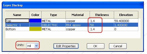
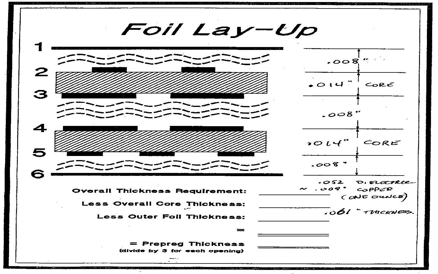
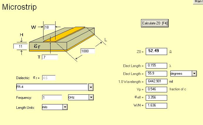
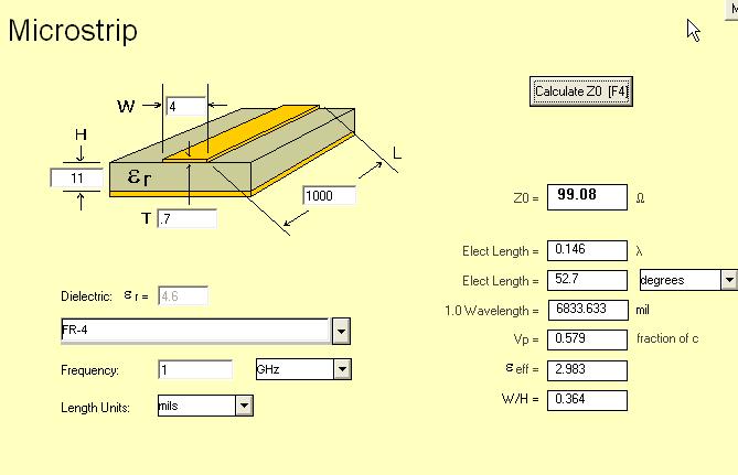
I'm doing a PCB design with a Microprocessor & few DDR2 667MHz. The recommended layer stack up was TOP, GND, INN1, INN2, VCC, BOTTOM. Can you recommend thickness of the board(prepreg and conductor layers? Impedances from the board are 50 & 100ohms.


Also what will be the drill pairs from my board. I'll be using blind & buried vias.

Thanks


see file for information, but you should ask your board manufacturer for specific build-up.
 

Hi bert_kak,

Can u show me the answers to ur query and how to get the values of thickness?

Please help me.

Thanks and Regards,
Tenny Thomas
 

Hi Bert,
Every layouter has exact to calculate the cooper with for hes PCB, but in accordance of the PCB producer to know what kind of cores & so stuckups are possible for you.
Than, if you can have i.e. 0.25mm core, you will calculate a cooper width of some tenth of mm for 100Ohm/ca.2x of that for 50ohm, & with these width have you to route all your impedance lines!
All others is-sorry a bungle...
In a car will you not fill "some fluid" and ask: will it go, how will it go, but you will fill some gasoline etc, also makes the right from beginning/start...
Good progress!
K.

Added after 57 minutes:

Btw,
If somebody needs the outer layers as impedance defined circuit, than is the, from loosemoose, proposed stackup inproper!
By that isnt garanted what kind of an Epsilon-rel. will have the outer layer (prepreg hase more epoxy, other "Er" value(!) as core & until/after thermal vacum pressing will be its thickness (epoxy-glass relation) not garantible & so the resulting impedance too....
For impedance defined outer layers you must order for that fix cores, & with the from you calculated thicknesses!
K.
 

hi bert,
i think it is not easy to achieve 100 ohm and 50 ohm in the same layer keeping a single referance plane.i think it ia better to go for different referance planes.
Still i tried with some stack ups eith 0.5 oz copper.
i used 11 mils as the distance from refeance layer
and got 18 mil tracewidth for 50 ohm and 4 mil width for 100 ohm. (refer the figures)


Hi Nikhil,

I heard that FR4-dielectric is not good for high frequency (gigahertz) because of loss.

Which software are u using to calculate the impedance?

-Tenny
 

appcad ..it is a free tool.. lot of people using it .

FR4 have some limitation when high frequency (upto gigahertz forget it) is considered .then we use some materials like arlon,Rogers etc.
 

NIKHILRAJ said:
hi bert,
i think it is not easy to achieve 100 ohm and 50 ohm in the same layer keeping a single referance plane.i think it ia better to go for different referance planes.

It is no problem to generate different impedance lines in the same layer using the same ground plane - you simply draw different width tracks.

Keith
 

hi keith,
here Bert need a 50 ohm and 100 ohm lines, when I calculated with 0.5 oz copper thickness and 11 mil gap from referance plane i got 18 mil trace for 50 ohm and 4 mil trace for 100 ohm. ( Can you please check the reliability of the data i got!!)
Bert is planning to route DDR and some signals from processor so will a 18 mil width tack ok for him?
or can you suggest a better layer stackup and trace widths?
 

This is a typical layer stackup for 6 layer:

https://www.pcb-pool.com/download/spezifikation/eng_cmso004_ml6.pdf

That would give 0.34mm wide for 50 ohms & 0.06mm width for 100 ohms on the top layer. So a layer with thicker dielectric would be required for the 100 ohm tracks.

Using layer 2 as ground plane and putting tracks on layer 3 would require around 0.125mm for 100 ohms which is just within their capabilities. Other PCB suppliers I am sure can do finer tolerances.

Keith.
 

Hi Keith,
Be care pls, as I wrote it some earlyer; its not right to have a prepreg construct between Layer 1/2 & 5/6, especially if its a so sensitive circuit as impedance defined & delay time uniformized layout as for DDR2/3 will needed!
As said, prepreg has not a 4.6-4.8 Epsrel, and their end value is less garanted as by cores! :-(
It will be really wrong for a DDR PCB...
Regards!
K.
 

Karesz,

I am sure you are right,

I normally do high speed analog & RF PCBs, not digital, but I think DDR PCBs would use more than 6 layers.

Keith
 

thanks for all your reply. after lots of studying and searching I found a decent software that answered my problems. I used SB200 from Polar & you define the PCB stack up & it calculates the line width for a certain impedance in a certain layer. It is a very good tool but I want other software so that I can compare the outputs to SB200. But another problem is i'm using this SB200 to compute for 75ohms impedance controlled line of composite video but the software doesn't give me correct results based on the designs i saw, it usually results to very small line width. Does analog signal have different consideration when it comes to line width?
 

I am still in confusion.....:!:
kieth,
can we fabricate narrow tracks with 0.06mm (I heard fabricator need a mininum trace width of 0.88 mm( 3.5 mils) .But it is expensive.
Is it important the number of layers of the PCB while calculating impedence of a trace. i think it is not the number of layers buth the distance from the referance plane is important .
 

NIKHILRAJ said:
I am still in confusion.....:!:
kieth,
can we fabricate narrow tracks with 0.06mm (I heard fabricator need a mininum trace width of 0.88 mm( 3.5 mils) .But it is expensive.
Is it important the number of layers of the PCB while calculating impedence of a trace. i think it is not the number of layers buth the distance from the referance plane is important .

i haven't talk to a manufacturer that can fabricate 0.06mm. but 0.8mm is common. number of layers is not important. its always the distance from the reference plane. hope this helps.
 

NIKHILRAJ said:
I am still in confusion.....:!:
kieth,
can we fabricate narrow tracks with 0.06mm

While it may be possible, it is not normal. If you end up with calculations which result in such thin tracks then you need another solution. The reason I suggest more layers is so you can have more choice of thickness to ground plane. However, if the 100 ohms tracks are differential not single ended then the calculations are incorrect.

Keith
 

The Simple PCB Impedance Calculator, PCB Stackup Impedance Calculator and
Trace Current Calculator are available in this link - **broken link removed**.

These are useful for automatic calculation of impedance and core/prepreg thickness.

In appcad, dual stripline trace calculator is not available.
 

Guys any idea on how much line width will I use for a 75ohms composite video signal? Thanks
 

Status
Not open for further replies.

Part and Inventory Search

Welcome to EDABoard.com

Sponsor

Back
Top