Continue to Site

Welcome to EDAboard.com

Welcome to our site! EDAboard.com is an international Electronics Discussion Forum focused on EDA software, circuits, schematics, books, theory, papers, asic, pld, 8051, DSP, Network, RF, Analog Design, PCB, Service Manuals... and a whole lot more! To participate you need to register. Registration is free. Click here to register now.

380V to 18V buck converter, troubles simulating

Status
Not open for further replies.
ERROR(ORPSIM-15157): |VON - VOFF| too small for VSWITCH model X_U3.xinsttl494.MSWITCH8.

ERROR(ORPSIM-15157): |VON - VOFF| too small for VSWITCH model X_U3.xinsttl494.MSWITCH7.

ERROR(ORPSIM-15157): |VON - VOFF| too small for VSWITCH model X_U3.xinsttl494.MSWITCH104.

ERROR(ORPSIM-15157): |VON - VOFF| too small for VSWITCH model X_U3.xinsttl494.MSWITCH101.

ERROR(ORPSIM-15157): |VON - VOFF| too small for VSWITCH model X_U3.xinsttl494.MSWITCH102.

ERROR(ORPSIM-15157): |VON - VOFF| too small for VSWITCH model X_U3.xinsttl494.MSWITCH103.

Are the errors when I change RELTOL from 0.001 to 0.1, convergence errors as you ramp the value up to 0.01

When I change ABSTOL, even from 1n to 1u, the convergence errors are still there.
 

There are a bunch of other simulation parameter limits. Did you change those also?

Otherwise I'm rather out of suggestions to help with the convergence.:sad:
 

Is there any way you could try to simulate a tl494 with what you have? If you've been doing that, I appreciate the time you've taken to do so already.

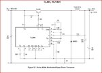
Perhaps you could walk me through this circuit? I'm curious to see if I have just wired the tl494 incorrectly into the base of the BJT. They use a PNP but I feel like it should be pretty straight forward. I'm not 100% on the use of the 47 ohm and the 150 ohm resistors either.

httpimg142.imageshack.usimg1424660fig2fy8.jpg
 

No, I'm using LTspice and unfortunately it doesn't have the TL494 in my part library.

I believe you are driving the buffer circuit properly. The circuit you show drives the pass transistor directly, which can be done as long as the supply voltage is no greater than the voltage rating of the TI494. The 47 ohm resistor is mainly to provide a faster turn-off for the transistor and the 150 ohm resistor is just to control the value of the base current to the pass transistor.

P.S. I'm done for the night. Likely be back in 7 hours or so. Cheers.
 

When a diode and coil are in contact, I have seen them create a rapid oscillating action in simulation.

1) The diode stops conducting.
2) The coil generates a spike,
3) Causing the diode to conduct briefly.

This occurs at each cycle. The simulator bogs down as it tries to reach convergence.

To cure this, I find it helps to install a resistor across either the coil or diode, or from their junction to ground, etc.
 

Well, after spending a few hours messing with error messages and trying to get rid of them by adding resistors around the circuit as a whole I got down to just 2 currents that do not converge:

These supply currents failed to converge:

I(X_U3.xinsttl494.Ev103) = -36.90nA \ -110.41pA
I(V_V2) = 1.967uA \ 95.04nA

These devices failed to converge:
Q_Q3 Q_Q4 X_U3.xinsttl494.X_U3.X1.Q1 X_U3.xinsttl494.X_U3.X2.Q1

Is all that I'm getting now. Below is a picture of the updated circuit. I found the "auto converge" option and it seems to be helpful in diagnosing the problems.

Updated.PNG

If I could figure out why Q3/Q4 aren't converging/switching properly I think my circuit is officially solved.

Edit: So after some more trial and error. I've gotten it down to

These supply currents failed to converge:

I(X_U3.xinsttl494.Ev103) = -22.00nA \ -110.51pA
I(V_V2) = 3.075uA \ -9.307nA

These devices failed to converge:
Q_Q3 Q_Q4

And based on the current values at each base of both Q3 and Q4. I can safely say Q3 is turning on and off like it is supposed to. However, I'm not getting the proper amount of current to turn on/off Q4. This then keeps my MOSFET from switching off all the way, so it really never bucks a voltage down :(

Pictures of the graphical results when I allow it to auto converge (to see what will happen)

Current into Q3
Q3.PNG
Current into Q4
Q4.PNG
Voltage on the source end of the MOSFET
Mos.PNG
Voltage as seen across rload
rload.PNG
And obligatory new circuit
New circuit.PNG
 
Last edited:

To make the N-mosfet shut off, it often helps to give its gate a more definite connection to ground or to its source pin, through a resistor.

10k is the value typically advised, so as not to interfere with it turning on fully.
 

I actually like that idea a lot, and I think this is what you had in mind.

Try4.PNG

This is the output now across rload

output.PNG

I still have convergence issues when I don't run the simulation with "Auto Converge" on. I'm afraid to bread board this to do physical load testing since it still doesn't converge properly in PSPICE.

Any ideas? With the set up as above, the things that aren't converging are as follows:

These voltages failed to converge:

V(X_U3.xinsttl494.102) = 178.73mV \ 181.01mV
V(X_U3.xinsttl494.101) = 178.73mV \ 181.01mV

These supply currents failed to converge:

I(X_U3.xinsttl494.Ev103) = -96.50nA \ 5.941nA
I(V_V2) = -7.925mA \ -10.19mA
I(X_U3.xinsttl494.VV51) = -1.186mA \ -1.200mA

These devices failed to converge:
D_D3 M_M2 Q_Q3 Q_Q4
 

When you see kV-range node voltages in a convergence
failure, that tends to implicate one of the models - likely
a "blowup" behavior at some V, I point outside where you'd
apply the device. There are functions that limit and there
are functions that blow up at extremes (or zero) and a
well crafted model will use limiting (or linear at the extrema)
functions.

Since the blowup value is inside the TL494 macromodel
this is a good way to bet - lousy with controlled sources
no doubt. Whether you're up for fixing it, or maybe just
want to take a closer look at how the macro may be
getting abused (like, just -maybe- it responds poorly to
380V on the supply, the output, or whatever), you may
be able to kill the nonconvergence by better care &
feeding - regulated supply, series limiting resistance on
outputs, clamps on inputs, whatever....
 

Why are you looking at ns waveforms? The switching period should be in the µs region.

How did you derive those oscillator values for R19 and C5? According to the data sheet they should be around 0.01µF and 8kΩ for oscillations in the 20kHz range. What frequency were you shooting for?

R18 in your latest circuit will significantly slow down the turn-on of the MOSFET. If you are adding that to improve convergence, use a value no larger than 100Ω.

You do not need or want any resistor from the MOSFET gate to ground as suggested by Brad. The MOSFET is rapidly turned off by Q3 through diode D2.

I believe you previous simulation of the driver circuit by itself worked okay, did it not? If that's the case then you shouldn't need to change anything in that part of the circuit.
 

All of my waveforms are in the ms region, not the ns (unless that was a typo, easy to do). I was just looking for a the reason why my mosfet wasn't shutting off all the way and by looking at those waveforms I could tell that the current at the base of Q4 was dropping at the same time the mosfet quit shutting off all the way.

R19 and C5 are the RT and the CT of the TL494. f = 1/(RT*CT) I believe. I was originally at 20k, but I thought at one point I may have been switching too quickly for Q4 to turn on/off fast enough, which in turn was causing the MOSFET to not shut off all the way. Turns out I was wrong about that. However, when I try to run it back at 20k, the simulation overloads in "auto convergence"


The MOSFET is currently failing to turn off all the way. The 10kohm resistor he suggested fixes that problem, but I'm guessing not for the right reasons?

So I made the changes you suggested. Ran the circuit in auto convergence mode (still doesn't quit come together otherwise) and I get a beautiful Vout

Perfect!.PNG

And the circuit, because why not

Hooray!.PNG
 
Last edited:

My mistake. The time markers were slightly blurry and I misread ms for ns.

The values you chose for R19 and C5 are outside the recommended range of values as shown in the chart (Figure 3 in my ON Semiconductor data sheet) of frequency versus timing resistance. It would be better to use 0.01µF and 5kΩ.

So it's working okay now? If you need to run it in the auto convergence mode, I see no problem with that. It should still give proper simulation results.

To speed up the transistor Q3 add about a 1nF capacitor in parallel across R28.
 

I've got the ideal circuit breadboarded to make sure everything is ok with a function generator before attaching the TL494 to it. I'm taking a break from the stress of trying to get this to work and writing parts of the paper that is going to accompany this project. I've been up since 6 yesterday with the sole focus of making it work. The pspice simulations are satisfactory enough for me to brave the bread board. I cannot begin to thank you enough for all the help you've given me, not to mention all the knowledge I've gained. I'll probably do testing in about an hour or 2, and hopefully have the load testing done with the whole circuit in 3-4 hours. I'll report back to post results and mark it as solved if everything works out like it's supposed to! Thank you so much again!

Something isn't working properly on the breadboard. The TL494 isn't behaving the way it's supposed to behave. After 4 hours of trying to troubleshoot problems I feel like my project is doomed.
 
Last edited:

.................................

Something isn't working properly on the breadboard. The TL494 isn't behaving the way it's supposed to behave. After 4 hours of trying to troubleshoot problems I feel like my project is doomed.
I've often spent many hours if not days trying to get a breadboard to work so it's not unusual to not find the problem after 4 hours. Does the TL494 work at all? Have you double checked all the wiring and component values? Have you measured all the pin voltages and see if they seem correct?

Troubleshooting is rather like a detective story. You look at all the clues and try to determine what's the most likely culprit. :wink:
 

Can you get a volt reading at the node joining the mosfet/ diode/ coil?

When the mosfet conducts, that node jumps to 32V.

You need to apply a higher gate voltage, to make the mosfet turn on fully.
 

You need to apply a higher gate voltage, to make the mosfet turn on fully.
I presume, you didn't realize the operation of the bootstrap driver.

Something isn't working properly on the breadboard. The TL494 isn't behaving the way it's supposed to behave. After 4 hours of trying to troubleshoot problems I feel like my project is doomed.
Did you change the oscillator components to the leagal range according to the datasheet?
Disabling the second error amplifier by shorting both inputs to ground is not supported by the specification. A differential voltage has to be applied.

Although it's a simple circuit, needing several hours to get it right isn't unusual. The problem may be that you didn't calculate the effort realistically.
 

In case you find it necessary to try a different driver than your TL494...

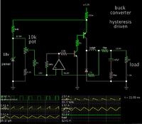
Here is a control circuit using an op amp, driven by hysteresis...


I gave the op amp an 18V supply (invisible), because your original spec was for 18V, and the op amp inputs should not be exposed to a greater amplitude than its supply V.

The small resistances are 'token' values.
 

Fvm is correct. To disable the second error amp you need to apply a positive voltage to the (-) input. That error amp is normally used for current limiting (as shown in Figure 21 of the ON data sheet) which you don't have.

Also, concentrating on just getting the circuit functioning, I didn't notice you don't have any compensation components (the 1megΩ, 47kΩ, and 0.1µF in Figure 21). The loop won't be stable without those. Those comp values are for the 1mH and 550µF output LC so your LC values would require different comp values. I think reducing the comp capacitor value to about 2.1nF should work for your values. You'd have to increase your output capacitor to 3900µF to give the same LC time-constant to work with those given comp values.

Here is a paper on how to design control loop compensation networks. View attachment Designing Stable Control Loops- TI.pdf
 

Apologies about being MIA for a bit, between the internet going down at school and trying my best to get the circuit functioning I haven't been back at the computer in a while.

I'm looking through the paper now. I fixed the wiring to the second error amp. I've added in the compensation components. I just need to do the calculations for them.

- - - Updated - - -

Also: I was pretty sure the output of my TL494 was the cause of the of the problem last night. (although at this point I have no idea) I wired it up by itself in a simple config shown below, and I'm aware that the input/output transistors are wired differently than what I need. I just wanted to test the output waveforms I was getting.

tl494 solo.PNG

and I get a resulting waveform of 12V peak to peak but it's centered around 0. In all the simulations I get a waveform that goes from 0-12V. This would greatly effect the rest of my circuit if I'm really putting in a square wave centered around 0, would it not? I'm pretty sure the BJTs aren't meant to have -6v pushed into the base.

Edit: How can I force the TL494 to give me a zero to some amount of voltage waveform? Is there a chip that I can replace the TL494 with in the future that will give me the waveform I'm looking for? (If my project fails to come together by 8am tomorrow I need to be able to at least suggest an easy solution that will avoid the problems I'm occuring now when someone new takes over the project. Assuming I'm given the pass to graduate tomorrow morning)
 

Status
Not open for further replies.

Part and Inventory Search

Welcome to EDABoard.com

Sponsor

Back
Top