Continue to Site

Welcome to EDAboard.com

Welcome to our site! EDAboard.com is an international Electronics Discussion Forum focused on EDA software, circuits, schematics, books, theory, papers, asic, pld, 8051, DSP, Network, RF, Analog Design, PCB, Service Manuals... and a whole lot more! To participate you need to register. Registration is free. Click here to register now.

QFN with exposed pad stencil opening

Status
Not open for further replies.

jgabcgr

Newbie level 4
Joined
Feb 11, 2017
Messages
7
Helped
0
Reputation
0
Reaction score
0
Trophy points
1
Activity points
68
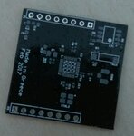
I made a pcb with a QFN32 with exposed pad but I feel like I've made a mistake on the stencil, in the exposed pad area. I managed to solder it and the chip (CC1310) is programmed successfully but I'm still concerned about the stencil. The solder paste looks like a chess on the exposed pad and I don't think that this is the right pattern. 7H81X.jpg
 

Hi,

The solder paste doesn't look that bad,
I'm surprised because of the solder stop.

Can you show us which recommendation you followed.

Klaus
 

I read once that the solder paste must be placed carefully in a way that it does not flow through the vias.
And I thought that if I placed solder mask on the vias it would stop the solder flowing. But unfortunately I follow the same thought on the stencil as well.
In a prompt search on the internet I read that some people use that guide of tented vias.
Fortunately the chip is programmed successfully but I haven't checked the radio part yet.
 

Hi,

I don't see any vias..

Klaus
 

There are 9 vias on the exposed pad, tented with squared solder paste.
 

So there's not me who see that the exposed pad has too little solder paste in contrast to the others package's pads. Eventually I figured out that there was not good idea to tent the vias, but how can we prevent the solder flowing through the vias if these aren't tented? How could I do that in this design?
 

Different implementation methods for thermal vias have their pros and cons, see this recent thread: https://www.edaboard.com/threads/365046/

Solder paste patterns are used to reduce the solder amount for large pads. In the present design, it looks like the QFN pads get potentially too much solder (paste pad reduction may be suitable) and the exposed pad too little. Can be better determined after reflow.

A low power IC like the RF transceiver can however tolerate some voids in the exposed pad soldering because heat dissipation is small (< 100 mW). A low inductance electrical connection will be achieved with little solder anyway. Would be more critical for switch mode converters or power transistors.

- - - Updated - - -

I believe the thermal pad solder will work well for CC1310.

but how can we prevent the solder flowing through the vias if these aren't tented? How could I do that in this design?
You don't necessarily need to prevent it absolutely, review the quoted application note in the linked thread.

One possible strategy is to make the thermal vias so small, that the drained solder amount is sufficiently low. If you look at the design of commercial PCBs, that's a frequently implemented option.

There's one absolute contraindication for solder wicking vias, that's double side reflow solder with exposed pad components assembled in the first pass. Then you get solder protruding conflicting with solder screen printing for the second pass. Via tenting or plugging required in this case.

There's also a certain possibility that solder wicking pulls down the QFN component and causes shorts on the outer pads.
 

Do a search for...
"bottom terminated components"
and
"IPC-7093"
Plent of relevant info out there. You need to aim for 50-70% of the solder void free at least, less voids is better.
 

Status
Not open for further replies.

Part and Inventory Search

Welcome to EDABoard.com

Sponsor

Back
Top