Welcome to our site! EDAboard.com is an international Electronics Discussion Forum focused on EDA software, circuits, schematics, books, theory, papers, asic, pld, 8051, DSP, Network, RF, Analog Design, PCB, Service Manuals... and a whole lot more! To participate you need to register. Registration is free. Click here to register now.
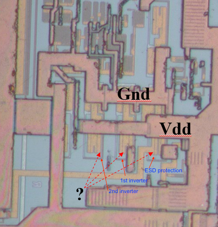
Hi, I would like to know the schematic and function of the layout shown in the below figure. Briefly.
it is probably an input buffer of CMOS logic circuit. But it seems to be slightly different from the MOS device I know.
What is it? please let me know.
Looks a bit "busy" to be just an input buffer, but it
could be that it's a general purpose bidirectional pad
call configured as an input. Then you have the output
buffer circuitry as well, tri-stated under logic control
(or tied off to rail at the output enable pin).
Some logic families were done "mini-array" style and
every signal pad was a general purpose I/O cell, mask
personalized at top (or sole) metal level.
I attached the detailed layout. The bottom part is definitely MOS, but i don't know what the part on the top meas. What is it??? it is an input stage of inverter.
- - - Updated - - -
Um... thank you, please look at the relpy below. I attached the detailed layout
This site uses cookies to help personalise content, tailor your experience and to keep you logged in if you register.
By continuing to use this site, you are consenting to our use of cookies.