Continue to Site

Welcome to EDAboard.com

Welcome to our site! EDAboard.com is an international Electronics Discussion Forum focused on EDA software, circuits, schematics, books, theory, papers, asic, pld, 8051, DSP, Network, RF, Analog Design, PCB, Service Manuals... and a whole lot more! To participate you need to register. Registration is free. Click here to register now.

S Parameter analysis for Cross coupled lc oscillator

Status
Not open for further replies.

W_ww

Newbie
Joined
Nov 26, 2015
Messages
5
Helped
0
Reputation
0
Reaction score
0
Trophy points
1
Activity points
45
Hello,

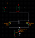
I am trying to do S parameter analysis for cross coupled LC oscillator. The first step is to analysis cross-pairs.
I want to get the gm and C. However, I have no idea that how to set up the test schematic, since for this, there is no input.
How can I set two ports?

Hope somebody can help me. Thanks in advance.

Best regards,
Wang
 

Attachments

  • Schematic.png
    Schematic.png
    12.3 KB · Views: 131

There isn't second port.The VCO has two parts, active part and passive part.If you obtain sufficient negative resistance from active side, you design a resonator in according with this active portion the VCO starts to swing..

Your test setup is completely wrong, the transistors are not biased at all.
Read something about VCO simulation techniques in Cadence help or on the internet..
 
  • Like
Reactions: W_ww

    W_ww

    Points: 2
    Helpful Answer Positive Rating
Thanks very much. But the schematic is not for the VCO, it is just S-parameter for active part to get the impedance. However, I think I was wrong, I also need the LC tack for the simulation.
 

Thanks very much. But the schematic is not for the VCO, it is just S-parameter for active part to get the impedance. However, I think I was wrong, I also need the LC tack for the simulation.
You should do the followings being as first steps..


-Change your s-parameter simulation setup accordingly within Cadence examples, don't use balun or such unnecessary components.Connect the port differentially via ideal blocking capacitors and Don't forget to supply the transistors via ideal chock coils. Your setup is therefore wrong...there isn't drain/collector supply
-Check your negative resistance coming from the active part and be sure that becomes at least 2.5 3 times higher than the magnitude of equivalent resistance of the resonator.Adjust the current in according within this..( current and transistor sizes,other stuffs until it's satisfied at every condition such as temperature,process variation etc)
-Then connect your resonator and set all the supplies up well then simulate it in a Cadence's HB or PSS simulation environment.
 

why do you bother with s parameter ?

just try to calculate your gm roughly gm = 2ID/Vov

then for oscillation it should satisfy this gm.Rp > 1

what is Rp ?

you have an inductor L and you know its Q so:

Rp= Q.L.W
 

Thanks for your reply. I almost finish design, and it works well in transient domain and I will do some analysis then.
Since it works at high frequency, I do the s-parameter analysis first.
But after several day's simulation, i am confused now. One question, negative resistance from the active part is more than 3 times than the resistance of LC tank. With Y-parameter analysis, active conductance Ga=1/re{Y11} should be less than 1/3 times of the LC conductance Gp (Gp=1/re{Y11}), right?
 

Status
Not open for further replies.

Part and Inventory Search

Welcome to EDABoard.com

Sponsor

Back
Top