sps101
Newbie level 6
Hello,
I am working on a project to design a 4-bit Flash ADC for a digital transceiver.The flash ADC should meet the following specifications:
Input frequency: 100MHz-500MHz
Sampling Rate: 2GS/s
VDD= 1.1V
signal voltage range = 0.5V peak-peak
I am using cadence with umc 65 technology.
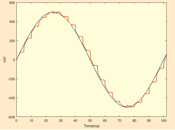
I am having a small issue when designing the sample and hold. I have used the open-loop architecture for fast switching and lower power. It is a mix of complementary input switch(NMOS AND PMOS) and a bottom plate switch as well.
I am getting some pedestal errors and sampling errors(error between original signal and sampled signal at the instant of sampling). I would like to know what is the acceptable range for the pedestal and sampling errors. Also, is there a way to reduce these errors ? The max pedestal error i am getting is 18mV. Max sampling error is 15mV


I am working on a project to design a 4-bit Flash ADC for a digital transceiver.The flash ADC should meet the following specifications:
Input frequency: 100MHz-500MHz
Sampling Rate: 2GS/s
VDD= 1.1V
signal voltage range = 0.5V peak-peak
I am using cadence with umc 65 technology.
I am having a small issue when designing the sample and hold. I have used the open-loop architecture for fast switching and lower power. It is a mix of complementary input switch(NMOS AND PMOS) and a bottom plate switch as well.
I am getting some pedestal errors and sampling errors(error between original signal and sampled signal at the instant of sampling). I would like to know what is the acceptable range for the pedestal and sampling errors. Also, is there a way to reduce these errors ? The max pedestal error i am getting is 18mV. Max sampling error is 15mV