Continue to Site

Welcome to EDAboard.com

Welcome to our site! EDAboard.com is an international Electronics Discussion Forum focused on EDA software, circuits, schematics, books, theory, papers, asic, pld, 8051, DSP, Network, RF, Analog Design, PCB, Service Manuals... and a whole lot more! To participate you need to register. Registration is free. Click here to register now.

MCP1642B voltage output problem, Sgnd and Pgnd pins

Status
Not open for further replies.

Ser35

Newbie level 4
Joined
Dec 28, 2015
Messages
7
Helped
0
Reputation
0
Reaction score
0
Trophy points
1
Activity points
85
Hello,

I am having a problem with the "MCP1642B - ADJ boost converter, in that it is not giving the 5V it is supposed to give: it sits at 4 Volts.

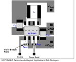
I built the circuit as in the Typical Application example, or also Figure 6.1 from the same datasheet (Figure 6.1 "Portable USB Powered by Li-Ion").

Here are my component values:

Cin = Cout = 47µF

L = 4.7µH

Rtop = 976 KΩ

Rbot = 300 KΩ

Vin = 3.3 V (from a step-down converter)

Rpull-up = 1 MΩ between the Vout pin and Power Good - PG - pin.

One thing that I noticed is that if I ground ONLY the "Sgnd" pin, the Vout is as calculated based on the resistor values and the vFB of aprox 1.21 V.

But if both the Pgnd and Sgnd are grounded, connected at the same GND node, then the output is 4V and no more.


Any suggestions with the same, or similar devices, are appreciated.
 

a simple sketch of your connection will help identify the problem.

Where did you connect EN pin of the IC?
 

also sounds like you may have a noise issue , with high di/dt current pulses going through your control ground.
The source sense res ground pad needs to be your control gnd.....star connect that to the chip ground so they are one and the sane at all times....don't let power switching current run through lengths of control ground.
You may also need to increase the series resistor going to the fet gate
 

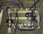
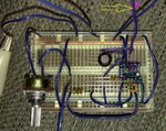
Hi, below I have attached a couple of pictures.

The EN is connected to Vin.

About the noise, I guess I cannot do much. Yes, I read about the Pgnd and star connections, which is new to me.

Most likely is to route "digital gnd or sgnd" pin through one line, "pgnd or agnd" pin through a different line, and connect both lines at the gnd of the power supply or battery (correct me if I am missing something or wrong).


treez:
"You may also need to increase the series resistor going to the fet gate"

Could you explain a bit more please?

Here is some other information:

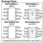
The package is 8MSOP, and it is soldered to a 8MSOP-to-DIP breakout adapter.

The circuit will be deployed in a perforated board. In the meantime, a breadboard is used for testing.

The source Vin comes from a step-down converter from 4xAA batteries to 3.3V from the target circuit.


I found in earlier models that the Sgnd and Pgnd must be attached externally, only if the package is 2x3 DFN.

The datasheet for the MCP1642B does not mention it (the 2x3DFN package condition).

From MCP1642 B/D:

3.6 Power Ground Pin (PGND)
The power ground pin is used as a return for the high-current N-Channel switch. The PGND and SGND pins are connected externally.

3.7 Signal Ground Pin (SGND)
The signal ground pin is used as a return for the integrated VREF and error amplifier. The SGND and power ground (PGND) pins are connected externally.

and

From MCP1640 B/C/D :
3.7 Signal Ground Pin (SGND)
The signal ground pin is used as a return for the integrated VREF and error amplifier. In the 2x3 DFN
package, the SGND and power ground (PGND) pins are connected externally.

3.8 Power Ground Pin (PGND)
The power ground pin is used as a return for the highcurrent N-Channel switch. In the 2x3 DFN package, the
PGND and SGND pins are connected externally.

Regards


inside_mcp.jpgpkg_mcp.jpgschematic_mcp.jpg

I forgot to mention: I used a multimeter to test the Sgnd and Pgnd for continuity, and it seems that they are connected internally with the 8MSOP.
 
Last edited by a moderator:

Hi,

I think it is a wiring problem. Either by completely wrong connection, or jusg not folowing the design rules for those switching power applications.

if I ground ONLY the "Sgnd" pin,
This sentence is scaring me. It means to me that (maybe only fof a short time) PGND was not connected.
This could immediately destroy the IC.

You need a proper PCB layout and proper device selection.
Simply connecting the parts like the schematic says does not work here.
Follow the design rules given in the datasheet. Read application notes and layout considerations.

Klaus


Klaus
 
  • Like
Reactions: Ser35

    Ser35

    Points: 2
    Helpful Answer Positive Rating
Could you explain a bit more please?
ok, now you've posted schem, I can see that you don't have a low side sense resistor, so please ignore my comment
 
  • Like
Reactions: Ser35

    Ser35

    Points: 2
    Helpful Answer Positive Rating
KlausST, thanks for your help.

For the moment I cannot generate a PCB just for the IC. I do not have the required tools :(. I have to work with a breadboard and hookup wires. Which means that I cannot come up with a GND copper layer, only wires.

Assuming a resistive load between 1K and 10K, if I connect both SGND and PGND pins together (as in the datasheet layout) and route them to the GND node of the power supply (like 2xAA batteries), the output voltage will not be 5 Volts, based on the resistor values mentioned in the datasheet of the "MCP1642B ADJ".

It will give an output of 4 Volts ~ 4.12 Volts. The feedback voltage is around ~0.96 Volts, and not ~1.21 Volts.

So far I cannot find an explanation as why I do not get the proper output voltage based on the resistor values if the SGND/PGND pins are tied together.

I will reduce the length of the wires, move around the components, and apply a small cap between the Vout and FB pin to see if that helps. I know that a breadboard is not the best place for these kind of circuits, but is what I have.


Thanks


mcpA.jpg
 

Hi,

Show us a picture of your actual circuit, where we can see all the nodes.
I think it is the pgnd connection or the output capacitor connection.

Klaus
 

Hello Klaus,

Here I attached a picture of the circuit on the breadboard.

Update:

*I added a 15 pF capacitor between Vout and FB pins.

*Used a dedicated wire from PGND pin and connects to the GND of the power supply and not on the GND of the breadboard.

It turns out it randomly gives voltage outputs either ~3.9 V or ~4.8 V when it is turned ON, with the modifications mentioned above. Without them the output is between ~3.6 V and 3.8 V.

Something is preventing the IC to deliver the +4.8 V.

Ser35


a5.jpg
 

Hi,

routing (wiring) of a 1MHz swtiching regulator circuit is not just connecting the signals.

*****

Datasheet says:
"The feedback resistors and feedback signal should be
routed away from the switching node and the switching
current loop."

But you did exactely the opposite with the connection from 19e to 22f.

*****

datasheet says:
"When wiring the
switching high-current paths, short and wide traces
should be used."

You see the design example.
The wires/traces are max. 3mm in length. And if you route it to be 20mm you will see the signals get worse.
But with the breadboard you are more near 300mm than at 3mm.
--> Look at PGND. It needs to be Short! Short! Short!
--> A breadboard is not suitable for those high frequency power switching circuits.

*****
There are two critical circuits/situations with your switching regulator.
1) For a very short time the internal switch is closed and energy coming from C_in is stroed in the choke L. (green line)
2) Also only for a short time the internal switch is open and the energy stored in the choke is given to the output capacitor. (magenta line)

The battery is not suitable to handle the power pulses in that short time (high frequency). Therfore you need C_in.

SMPS1.PNG
In schematic the length of the lines are not critical, but in real circuit.

Now to your breadboard:
Again the two signal paths are shown:
SMPS2.JPG
green: It should be short, but it is much too long.
magenta: It is way too long. One can not even see how long it is and where it goes. It should be as short as possible.

Klaus
 
Last edited:
  • Like
Reactions: Ser35

    Ser35

    Points: 2
    Helpful Answer Positive Rating
Status
Not open for further replies.

Similar threads

Part and Inventory Search

Welcome to EDABoard.com

Sponsor

Back
Top