thiagofinottimoraes
Newbie level 6
Hello,
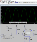
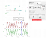
I have simulated on LTspice a very simple CE amplifier as attached - picture and .asc simulation.
No AC capacitor at the emitter, plain and simple CE emitter bias unbypassed, in this case gain is Av = -Rc / RE = 4.07.
It turns out that, as input is a perfect 1V sine, at Vout, negative swing reaches -3.82V, and positive swing goes to +4.11V. That is not so small to be disregarded.
Any ideas why negative swing doesn't reach its full value??
**broken link removed**
**broken link removed**