Continue to Site

Welcome to EDAboard.com

Welcome to our site! EDAboard.com is an international Electronics Discussion Forum focused on EDA software, circuits, schematics, books, theory, papers, asic, pld, 8051, DSP, Network, RF, Analog Design, PCB, Service Manuals... and a whole lot more! To participate you need to register. Registration is free. Click here to register now.

How to measure IIP3 and SFDR of a complex filter in spectre?

Status
Not open for further replies.

zf3177

Newbie level 4
Joined
Nov 12, 2015
Messages
7
Helped
0
Reputation
0
Reaction score
0
Trophy points
1
Activity points
120
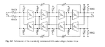
Hey guys, I just designed a active-RC complex filter based on TT biquad and work for GPS or Compass Receiver.
The filter has 4 ports include two in-phase and two quadrature inputs.
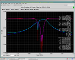
The in-phase consists of two AC signals, they are Mag 1.0 Phase 0.0 and Mag 1.0 Phase 180.
The Q-phase are Mag 1.0 Phase 180 and Mag 1.0 Phase 270
The similarity topics I had searched is not clear and many test methods based on LNA/Mixer, SFDR test often exists in DAC
Can somebody help me or provide some elaborate documents?
Thanks.
 

Attachments

  • Clipboard01.png
    Clipboard01.png
    101.1 KB · Views: 152
  • Like
Reactions: zf3177

    zf3177

    Points: 2
    Helpful Answer Positive Rating
Simply drive DUT by Iin or Iin_plus and Iin_minus.
Then measure Iout+j*Qout or (Iout_plus-Iout_minus)+j*(Qout_plus-Qout_minus).

Here you should use PSS/PAC

https://www.designers-guide.org/Modeling/modeling-rf-systems.pdf

Thanks for your reply, and the document you had uploaded is very useful and it must take some time to read.
And there still some trouble confused me.
First, In complex filter AC response test, I just test (Iout_plus-Iout_minus) but not include (Qout_plus-Qout_minus), In order to measure the expression you had provided "(Iout_plus-Iout_minus)+j*(Qout_plus-Qout_minus)", how to realize "j" in spectre?
Second, in cadence official simulator reference and some other documents.To test IP3 usually add two frequency in one AC sources as follows:

Choosing Analyses Form Select ac from the Analysis section.
At the bottom of the form, set Specialized Analysis to Rapid IP3. The form expands.
Select port for Source Type.
Select the Input Sources 1 field.
Click the Select button just above that field.
Select the Port source /RF at the left of the schematic.
Select Input Port
Type 900M in the Freq field to the right of Input Sources 1.
Type /RF in the Input Sources 2 field. (Alternately, you could select the RF port in the schematic by first clicking the Select button and then selecting the RF source in the schematic).
Type 920M in the Freq field the to the right of Input Sources 2.
Type -50 in the Input Power (dBm) field.
Type 940M in the Frequency of IM Output Signal field.
Type 900M in the Frequency of Linear Output Signal field.
Type /out1 in the Out+ field. Because you are leaving the Out- field blank, it will default to ground.
Leave the rest of the form at their default values. The Choosing Analyses form should look like the following:

The above words are quote from the method of Measuring IP3 with Rapid IP3 in cadence help document.And I don't know how to use it in the test of my complex filter.May be I should find the way to measure fully differential amplifier as reference?
 

In order to measure the expression you had provided "(Iout_plus-Iout_minus)+j*(Qout_plus-Qout_minus)", how to realize "j" in spectre?
Spectre is no more than classic Spice type simulator, so Spectre never can treat complex signal by only one wire and you can nevere realize "j" in Cadence Spectre.
Instead, complex signal is treated by two wires, Isig and Qsig.
Then you can construct complex signal Isig + j*Qsig as Post Processing.
The following is a example Skill Function which create complex signal over negative to positive frequency from only positive frequency data.
Negative frequency data can be constructed from positive frequecncy data, since I(-freq)=conj(I(freq)) and Q(-freq)=conj(Q(freq)).
Code:
procedure( bb_ac_probe(wfI, wfQ)
  let( (I_p, I_n, Q_p, Q_n, p, n, xvec_p, yvec_p, xvec_n, yvec_n, i, nlen)

    I_p = wfI
    I_n = flip( conjugate(I_p) )

    Q_p = wfQ
    Q_n = flip( conjugate(Q_p) )

    p = I_p + complex(0.0, 1.0)*Q_p
    n = I_n + complex(0.0, 1.0)*Q_n

    xvec_p = drGetWaveformXVec(p)
    yvec_p = drGetWaveformYVec(p)

    xvec_n = drGetWaveformXVec(n)
    yvec_n = drGetWaveformYVec(n)

    nlen = drVectorLength(xvec_n)

    for(i, 1, nlen-1
        drAddElem( xvec_n, drGetElem(xvec_p, i) )
        drAddElem( yvec_n, drGetElem(yvec_p, i) )
    ); for

    drCreateWaveform(xvec_n, yvec_n)
  ); let
); procedure

The above words are quote from the method of Measuring IP3 with Rapid IP3 in cadence help document.
"Rapid IP3" is very suspicious.
Even Cadence don't push advertisement of "Rapid IP3" recently.

And I don't know how to use it in the test of my complex filter.
If you want to evaluate Gain, use conventional AC analysis.
If you want to evaluate IP3, use PSS/PAC analysis where one signal is large signal for PSS and the other signal is small signal for PAC.
https://www.designers-guide.org/Analysis/intercept-point.pdf

May be I should find the way to measure fully differential amplifier as reference?
No.
Whether Single-ended or Differential has no relation to complex signal at all.
If you would like to treat differential signal as single-ended signal, use ideal balun.
https://www.designers-guide.org/Analysis/diff.pdf
Even if you use four baluns, input signals are consisted from two signals(Iin and Qin), also output signal are consisted from two signals(Iout and Qout).

Direct Plot of Cadence ADE can not be useful for complex signal.
You have to write your own OCEAN(SKILL) functions to do post processing for complex signal such as I+j*Q.
 
Last edited:
  • Like
Reactions: zf3177

    zf3177

    Points: 2
    Helpful Answer Positive Rating
Spectre is no more than classic Spice type simulator, so Spectre never can treat complex signal by only one wire and you can nevere realize "j" in Cadence Spectre.
Instead, complex signal is treated by two wires, Isig and Qsig.
Then you can construct complex signal Isig + j*Qsig as Post Processing.
The following is a example Skill Function which create complex signal over negative to positive frequency from only positive frequency data.
Negative frequency data can be constructed from positive frequecncy data, since I(-freq)=conj(I(freq)) and Q(-freq)=conj(Q(freq)).
Code:
procedure( bb_ac_probe(wfI, wfQ)
  let( (I_p, I_n, Q_p, Q_n, p, n, xvec_p, yvec_p, xvec_n, yvec_n, i, nlen)

    I_p = wfI
    I_n = flip( conjugate(I_p) )

    Q_p = wfQ
    Q_n = flip( conjugate(Q_p) )

    p = I_p + complex(0.0, 1.0)*Q_p
    n = I_n + complex(0.0, 1.0)*Q_n

    xvec_p = drGetWaveformXVec(p)
    yvec_p = drGetWaveformYVec(p)

    xvec_n = drGetWaveformXVec(n)
    yvec_n = drGetWaveformYVec(n)

    nlen = drVectorLength(xvec_n)

    for(i, 1, nlen-1
        drAddElem( xvec_n, drGetElem(xvec_p, i) )
        drAddElem( yvec_n, drGetElem(yvec_p, i) )
    ); for

    drCreateWaveform(xvec_n, yvec_n)
  ); let
); procedure

"Rapid IP3" is very suspicious.
Even Cadence don't push advertisement of "Rapid IP3" recently.

If you want to evaluate Gain, use conventional AC analysis.
If you want to evaluate IP3, use PSS/PAC analysis where one signal is large signal for PSS and the other signal is small signal for PAC.
https://www.designers-guide.org/Analysis/intercept-point.pdf

No.
Whether Single-ended or Differential has no relation to complex signal at all.
If you would like to treat differential signal as single-ended signal, use ideal balun.
https://www.designers-guide.org/Analysis/diff.pdf
Even if you use four baluns, input signals are consisted from two signals(Iin and Qin), also output signal are consisted from two signals(Iout and Qout).

Direct Plot of Cadence ADE can not be useful for complex signal.
You have to write your own OCEAN(SKILL) functions to do post processing for complex signal such as I+j*Q.

Thank you very much for give me so much help.
But I am not familiar with Ocean/Skill language, I had searched some document about how to programming and use this language to simulation there still some problem need you for help.

First,the complex filter process complex signals by using two wires and output two wires which you proposed Isig and Qsig, but after the signal processed by complex filter, We can obtain each of two wires of signal has same AC response, the signals can be demodulate by using Isig or Qsig but no need to construct(This was found in a post by someone).So, can't we simulate complex filters by only use Isig or Qsig?

Second,about the Ocean/Skill language.As I have no fundamental knowledge about this tool, I just list my comprehension about you code and all code use in simulate.
Code:
procedure( bb_ac_probe(wfI, wfQ)      
let( (I_p, I_n, Q_p, Q_n, p, n, xvec_p, yvec_p, xvec_n, yvec_n, i, nlen)

    I_p = wfI
    I_n = flip( conjugate(I_p) )   

    Q_p = wfQ
    Q_n = flip( conjugate(Q_p) )

    p = I_p + complex(0.0, 1.0)*Q_p    
    n = I_n + complex(0.0, 1.0)*Q_n

    xvec_p = drGetWaveformXVec(p)     
    yvec_p = drGetWaveformYVec(p)

    xvec_n = drGetWaveformXVec(n)
    yvec_n = drGetWaveformYVec(n)

    nlen = drVectorLength(xvec_n)

    for(i, 1, nlen-1
        drAddElem( xvec_n, drGetElem(xvec_p, i) )
        drAddElem( yvec_n, drGetElem(yvec_p, i) )
    ); for

    drCreateWaveform(xvec_n, yvec_n)
  ); let
); procedure
save_path=/home/username/Desktop/Polyphase_test_result/
simulator( 'spectre )
design( "/home/username/simulation/tt_polyphase/spectre/schematic/netlist/netlist")
resultsDir(save_path)
modelFile( 
    '("/home/username/Desktop/models/allModels" "")
)
analysis('dc ?saveOppoint t  )
envOption(
	'analysisOrder  list("dc")
)
temp( 27 ) 
run()
Here I infered:
In schematic view
I_p,I_n,Q_p,Q_n are 4 output ports. Filp & conjugate command used to find negative data.
p and n represents the Isig and Qsig.
using 4 vectors receive the data of p and n and finally construct complex signal.
The above codes can be directly used in spectre? Hope you can provide some detail simulate method documents based on skill language.
 

So, can't we simulate complex filters by only use Isig or Qsig?
It is simple math.
H = Hi + j*Hq
A = Iin + j*Qin
B = Iout + j*Qout

Hi, Hq, Iin, Qin, Iout and Qout are all complex value for AC and PAC analysis.

B = H * A = (Hi*Iin - Hq*Qin) + j*(Hi*Qin + Hq*Iin)

Iout = Hi*Iin - Hq*Qin
Qout = Hi*Qin + Hq*Iin

When Qin=-j*Iin(mag of Iin and Qin=1, phase of Iin=0deg, phase of Qin=-90deg), Iout=(Hi+j*Hq)*Iin. Qout=(Hi+j*Hq)*Qin
So H=Iout/Iin=Qout/Qin.

But I am not familiar with Ocean/Skill language, I had searched some document about how to programming and use this language to simulation there still some problem need you for help.
If you are not familiar with Ocean/Skill language, use your favorite language for post processing.
For example, you can use MATLAB directly to do post post processing PSF data of Cadence Spectre results.

https://www.lumerink.com/courses/ECE697A/docs/Cadence+Spectre+Matlab+Toolbox.pdf
 
Last edited:

It is simple math.
H = Hi + j*Hq
A = Iin + j*Qin
B = Iout + j*Qout

Hi, Hq, Iin, Qin, Iout and Qout are all complex value for AC and PAC analysis.

B = H * A = (Hi*Iin - Hq*Qin) + j*(Hi*Qin + Hq*Iin)

Iout = Hi*Iin - Hq*Qin
Qout = Hi*Qin + Hq*Iin

When Qin=-j*Iin(mag of Iin and Qin=1, phase of Iin=0deg, phase of Qin=-90deg), Iout=(Hi+j*Hq)*Iin. Qout=(Hi+j*Hq)*Qin
So H=Iout/Iin=Qout/Qin.

If you are not familiar with Ocean/Skill language, use your favorite language for post processing.
For example, you can use MATLAB directly to do post post processing PSF data of Cadence Spectre results.

https://www.lumerink.com/courses/ECE697A/docs/Cadence+Spectre+Matlab+Toolbox.pdf
Thanks for explain the problem with above equations!
Spectre simulation data processing in matlab can't used because the cadence software installed in linux and locked by our administrator.
For me, the ocean/SKill seems available.
In these day I had read the PSS/PAC and IIP3 measurement provided by you and cadence official document.
The most important problems is although I had got the detail simulate process and some simulate examples, I can't do nothing in my complex filter cause it has I and Q signal route and 4 input ports.
Sorry for my bad knowledge and skill, will you please provided some complex filter testbench or codes?
And I supposed that in your reply,the simulation method you had advised:
AC response simulation:
According the equation you had mentioned.To test either Isig or Qsig we can get the Gain and Phase in complex filter just set the input Iin Qin in certain value.
IIP3 or SFDR simulation:
This kind of simulations must insert the instance in spectre like "psin" to obtain HB or PAC/PSS simulation, and I don't know how to deal with complex filter with 4 ports.
As the "psin" has insert instead of ac signals,The equation "H=Iout/Iin=Qout/Qin" is no longer estabilished, then we need Skill language & Matlab to contruct a complex expression for process the simulation data, is that right?
 

will you please provided some complex filter testbench or codes?
Imagine actual measurement using actual instruments, not EDA Tool Play.
Simply do same set up in EDA Tool.
Gain and IIP3 can be evaluated even by Transient Analysis.

Show me your incomplete netlist regarding signal source definitions and analysis statements.
I can edit your incomplete netlist.

AC response simulation:
According the equation you had mentioned.To test either Isig or Qsig we can get the Gain and Phase in complex filter just set the input Iin Qin in certain value.
Yes.

IIP3 or SFDR simulation:
This kind of simulations must insert the instance in spectre like "psin" to obtain HB or PAC/PSS simulation
Correct. However, use "vosurce", neither "psin" nor "port".
And "analogLib/psin" is netlisted as "port" for Cadence Spectre.
Also "analogLib/vsin" is netlisted as "vsource" for Cadence Spectre.
Both "psin" and "vsin" don't exist in Spectre primitive.
See "spectre -h port" and "spectre -h vsource".

and I don't know how to deal with complex filter with 4 ports.
Still you can not understand complex signal at all.
DUT is no more than 2-input(I and Q) and 2-output(I and Q) system.

Ain=(Iin_p-Iin_m) + j*(Qin_p-Qin_m)
Bout=(Iout_p-Iout_m) + j*(Qout_p-Qout_m)
Bout = H * Ain, here H = Hi + j*Hq, Complex Gain is H.

Iin_p = 0.5, Iin_m = -0.5
Qin_p = -j*0.5, Qin_m = -j*(-0.5)

Simply reflect the aboves to "analogLib/vsource" for AC, PSS/PAC.
You have to set the aboves as large signal for master PSS analysis.
And set the aboves as small signal for slave PAC analysis.
For AC analysis, only small signal is required.

See my append #7 in https://www.edaboard.com/threads/169169/

As the "psin" has insert instead of ac signals,The equation "H=Iout/Iin=Qout/Qin" is no longer estabilished
Wrong.
Results of PSS(both Shoooting and HB) are Phasor.
https://en.wikipedia.org/wiki/Phasor

then we need Skill language & Matlab to contruct a complex expression for process the simulation data, is that right?
Little correct.
 
Last edited:

I just designed a active-RC complex filter based on TT biquad
For my filter center freqency=5.9MHz Bandwidth=4Mhz
zf3177 said:
pancho_hideboo said:
What scheme do you want to use as IP3 definition, voltage(dBV) or power(dBm) ?
power(dBm) is better...
Can you understand very basic concept surely ?
If you want to define Gain and IP3 as power, you have to define reference impedance for both input and output.
Input reference impedance is Signal source impedance.
Output reference impedance is Load impedance.
What value do you use as reference impedance ?

I think the reference impedance you refered is 50ohm or the impedance to drive next stage?
I don't think your circuit can work when you use 50ohm load.

Again surely study voltage(dBV) or power(dBm).
If you use former, you don't have to define signal source impedance and can use high impedance as load.
I don't think Gain and IP3 based on power definition are useful for active filter operated around 5MHz.

zf3177 said:
pancho_hideboo said:
What frequency do you use as two input frequency for IP3 evaluation ?
fin_1 amd fin_2 ?
freq1 freq2 I want to set:freq1=4.5MHz freq2=6.5Mhz and these two freq are all in band.
You can not understand IP3 at all.
IM3_L=2*freq1-freq2=2.5MHz, IM3_U=2*freq2-freq1=8.5MHz
Both IM3_L and IM3_U are outband.
Such IP3 is meaningless.

Center frequency of your filter is 5.9MHz.
BW of your filter is 4.0MHz.
So delta_f between freq1 and freq2 has to be far less than 4MHz/3=1333kHz.
For example, freq1=5.9MHz-100kHz=5.8MHz, freq2=5.9MHz+100kHz=6.0MHz, delta_f=200kHz.

Again show your netlist regarding signal source definitions and analysis statements.

I reject all personal message from you.
Instead, describe on this thread using correct terminology.
 
Last edited:

Hope you don't mind my carelessness behaviour and send persional massage disturbed you:)
And I hadn't test IIP3 in any other RF circuits before.I admit that my comprehension to this concept is not full.
So I need to test this filter as exercise but make many jokes.
First, the freq1 and freq2, according your guide. It is reasonable to choose freq1=5.8MHz and freq2=6.0MHz as you said.
So delta_f between freq1 and freq2 has to be far less than 4MHz/3=1333kHz
Why far less than 4MHz/3?
Again show your netlist regarding signal source definitions and analysis statements.
The netlist followed your requirment as follow include AC response analysis statements.For PAC or PSS simualte..I don't know how to do..
Code:
simulator lang=spectre
global 0 vdd!
include "/home/username/Desktop/models/allModels"

// Library name: FDRFC
// Cell name: FDRFC_Circuit_synbol
// View name: schematic
subckt FDRFC_Circuit_synbol GND VDD Vcmfb Vin\+ Vin\- Vout\+ Vout\-  
ends FDRFC_Circuit_synbol
// End of subcircuit definition.

// Library name: FDRFC
// Cell name: vcmfb_circuits_symbol
// View name: schematic
subckt vcmfb_circuits_symbol GND VDD Vcmfb Vout\+ Vout\- Vref
ends vcmfb_circuits_symbol
// End of subcircuit definition.

// Library name: FDRFC
// Cell name: FDRFC_ALL
// View name: schematic
subckt FDRFC_ALL GND VDD Vin\+ Vin\- Vout\+ Vout\- Vref
    I0 (GND VDD net17 Vin\+ Vin\- Vout\+ Vout\-) FDRFC_Circuit_synbol
    I1 (GND VDD net17 Vout\+ Vout\- Vref) vcmfb_circuits_symbol
ends FDRFC_ALL
// End of subcircuit definition.

// Library name: two_stage_opamp
// Cell name: tt_polyphase_6Mhz
// View name: schematic
RQT8 (net28 net070) resistor r=2.6K
RQT7 (net26 net071) resistor r=2.6K
RQT6 (net27 net073) resistor r=2.6K
RQT5 (net25 net072) resistor r=2.6K
RQT2 (net049 net066) resistor r=2.6K
RQT1 (net037 net067) resistor r=2.6K
RQT4 (net047 net068) resistor r=2.6K
RQT3 (net048 net050) resistor r=2.6K
RC8 (net28 Iout_m) resistor r=26.525K
RC7 (net26 Iout_p) resistor r=22K
RC6 (net25 Qout_m) resistor r=22K
RC5 (net27 Qout_p) resistor r=22K
RC4 (net047 net22) resistor r=22K
RC3 (net048 net17) resistor r=22K
RC2 (net037 net24) resistor r=22K
RC1 (net049 net19) resistor r=22K
RW8 (net047 Qout_p) resistor r=90K
RW5 (net048 Qout_m) resistor r=90K
RW6 (net19 net26) resistor r=90K
RW7 (net24 net28) resistor r=90K
RQ4 (net047 net24) resistor r=200K
RQ3 (net048 net19) resistor r=200K
RI3 (Qin_p net048) resistor r=80K
RI4 (Qin_m net047) resistor r=80K
RW4 (net049 Iout_p) resistor r=90K
RW1 (net037 Iout_m) resistor r=90K
RQ2 (net049 net22) resistor r=200K
RQ1 (net037 net17) resistor r=200K
RI1 (Iin_p net037) resistor r=80K
RI2 (Iin_m net049) resistor r=80K
RW3 (net22 net27) resistor r=90K
RW2 (net17 net25) resistor r=90K
V6 (vref 0) vsource dc=900m type=dc
V4 (vdd! 0) vsource dc=1.8 type=dc
V2 (Qin_p 0) vsource dc=900m mag=1 phase=90 type=sine
V3 (Qin_m 0) vsource dc=900m mag=1 phase=270 type=sine
V11 (Iin_p 0) vsource dc=900m mag=1 phase=0 type=sine
V9 (Iin_m 0) vsource dc=900m mag=1 phase=180 type=sine
I143 (0 vdd! net048 net047 net24 net19 vref) FDRFC_ALL
I133 (0 vdd! net037 net049 net22 net17 vref) FDRFC_ALL
I138 (0 vdd! net25 net27 Iout_m Iout_p vref) FDRFC_ALL
I140 (0 vdd! net26 net28 Qout_m Qout_p vref) FDRFC_ALL
CF8 (Qout_m net070) capacitor c=1p
CF7 (Qout_p net071) capacitor c=1p
CF4 (net24 net068) capacitor c=1p
CF3 (net19 net050) capacitor c=1p
CF6 (Iout_m net073) capacitor c=1p
CF5 (Iout_p net072) capacitor c=1p
CF2 (net22 net066) capacitor c=1p
CF1 (net17 net067) capacitor c=1p
simulatorOptions options reltol=1e-3 vabstol=1e-6 iabstol=1e-12 temp=27 \
    tnom=27 scalem=1.0 scale=1.0 gmin=1e-12 rforce=1 maxnotes=5 maxwarns=5 \
    digits=5 cols=80 pivrel=1e-3 sensfile="../psf/sens.output" \
    checklimitdest=psf 
ac ac start=-10M stop=10M annotate=status 
modelParameter info what=models where=rawfile
element info what=inst where=rawfile
outputParameter info what=output where=rawfile
designParamVals info what=parameters where=rawfile
primitives info what=primitives where=rawfile
subckts info what=subckts  where=rawfile
saveOptions options save=allpub
What value do you use as reference impedance ?
I don't know test IIP3 must use reference impedance as I had read carefully the document you had provided, may be I had missed something.
The input signal source impedance are't decided by simulation method?
For example:"Psin" is a instance in spectre which contain 50ohm impedance.
I don't think Gain and IP3 based on power definition are useful for active filter operated around 5MHz.
The circuit I had made and read many papers as reference..much of them use IIP3 as a parameter to test linearit, even in lower frequency.
Some of them use in band/out of band SFDR
 

Why far less than 4MHz/3?
To keep IM3_L and IM3_U inside bandwidth of your filter.

The input signal source impedance are't decided by simulation method?
No.
It has to be output impedance of former stage.

much of them use IIP3 as a parameter to test linearit, even in lower frequency.
I use IP3 defined by voltage(dBV).
I don't use IP3 defined by power(dBm), if I define IP3 for your filter.
Again can you really understand power and voltage ?

If you prefer dBm, what value do you use as reference impedance ?
For example, Rs=1kohm, Rload=500kohm

I can not use your netlist if you prefer IP3 based on power.

If you prefer IP3 defined by power(dBm), use "port" instead of "vsource" as input signals and place resistive loads for outputs.
Then show updated netlist.
 
Last edited:

Again can you really understand power and voltage ?
Of course I know :) but I just confused in the RF receiver chain.
I searched certain documents and get difference between them and I get new problems:
dBm used in receiver chain but having matched impedances like 50ohm.
But if receiver have mismatch impedance,but only the LNA has 50ohm(match impedance)input impedance, start using voltages/currents/impedances instead of powers is more suitable, right?
And according to your reply..it makes no sense to calc IIP3 without know the source/load impedance. Why so many paper displayed there IIP3 without showed there previous/next stage? I don't think they made a whole receiver chian..or simply set source/load impedance as 50 ohm?

If you prefer IP3 defined by power(dBm), use "port" instead of "vsource" as input signals and place resistive loads for outputs.
I prefer use source impedance 50ohm and next stage input impedance is infinite (gate of the nmos as input stage) so how to get Rload?
 

Of course I know
I can not think so.
Can you understand difference between Power Source Drive and Voltage Source Drive ?
Many people including you can not understand this very basic concept at all.
I've been always tired.
See the followings.
https://www.designers-guide.org/Forum/YaBB.pl?num=1266168115/1#1
https://www.designers-guide.org/Forum/YaBB.pl?num=1277737192/1#1

But if receiver have mismatch impedance,but only the LNA has 50ohm(match impedance)input impedance
I can not understand what you want to mean at all.

start using voltages/currents/impedances instead of powers is more suitable, right?
I can not understand what you want to mean at all.

If you stimulate DUT by Power Signal Source and input impedance of DUT is not matched to Signal source impedance, how do you know signal level at gate of MOS-FET ?
This is a reason why I use IP3 defined by voltage not power.

And according to your reply..it makes no sense to calc IIP3 without know the source/load impedance. Why so many paper displayed there IIP3 without showed there previous/next stage? I don't think they made a whole receiver chian..or simply set source/load impedance as 50 ohm?
See product data sheet, many IP3 are defined by voltage.
And see attached figure, there Rs=500ohm and Rload=500ohm.

I prefer use source impedance 50ohm and next stage input impedance is infinite (gate of the nmos as input stage) so how to get Rload?
Power Source Drive and observation of output voltage.
Direct Plot Form of Cadence ADE can treat only Power Source Drive and observation output power.

Before going to complex filter, learn very basic concept surely.

(1) Power Source Drive and Voltage Source Drive
(2) IP3 for real signal, e.g. IP3 for LNA
(3) IP3 evaluation for (2) using PSS/PAC
 

Attachments

  • 151201-003724.png
    151201-003724.png
    24.8 KB · Views: 136
Last edited:

Can you understand difference between Power Source Drive and Voltage Source Drive ?
I had seen your posted in many years before and read carefully.
And really appreciate your guidance.
After read your posted, in my opinion
Voltage Source Drive:A source provide voltage in input nodes and get output voltage in output nodes and obtain voltage gain by Vout/Vin(Vsource)
Power Source Drive:As you posted reply R.Zakai

As direct method, assume port impedances(=reference impedances), R01 and R02 are all real.
Available power of port1 is Pa=(|E|/2)2/R01
Power delivered to port2 is Pload=|V2|2/R02
|S21|^2=Pload/Pa=(2*|V2/E|)2*R01/R02
S21=(2*V2/E)*sqrt(R01/R02)=(V2/(E/2))*sqrt(R01/R02)
Here "E" is an open circuit voltage of port1. And E/2 is not equal to V1 generally.
S21 is different from conventional voltage gain V2/V1 even if R01 is equal to R02.
Also |S21|^2 is different from conventional power gain Pload/Pin.

About reference impedance..Still some problems comfused me.
One is signal impedance,another is input and output impedance of certain block.
I know the basic theory about input and output impedance of a circuit.
And in ultra/high frequency we should having matched impedances in order to corresponding signal source to maximize the power transfer or minimize signal reflection from the load.
So, in IP3 test, in order to let the signal impedance matching input impedance of circuits, set port res value equal to 50ohm (in your attached figure)? If not, why LNA test examples in cadence reference without know the input impedance of LNA but set port res value 50ohm arbitrarily?
In attached thumbnails I can understand the Rs=500ohm and the circuit need it to obtain the function of filter, but I don't think it is the output impedance of former stage.

Rload, in this paper, just set the value arbitrarily or equal to input impedance of next stage?

Before going to complex filter, learn very basic concept surely.

(2) IP3 for real signal.
I get the relevant knowlege in document "Accurate and Rapid Measurement of IP2 and IP3". In general:

The traditional approach to measuring a two-tone nth-order IMD intercept point, IPn, begins by applying two sinusoids to the circuit’s input at f1 and f2. Make the amplitude of the two sinusoids the same, and increase their power while plotting the power at the output in a fundamental (either f1 or f2) and in an nth-order intermodulation product (for IP3 use either 2f1 – f2 or 2f2 – f1)

(3) IP3 evaluation for (2) using PSS/PAC
IP3 is measured with a two-tone test. One tone is the fundamental PSS frequency while the other is the frequency in a single point PAC analysis
After read the test procedure of Mixer and LNA I considered the simulate procedure in complex filter:
First,set PSS analysis set port1:
in port1 set freq1= 5.8MHz and amplitude as variable "power" and res=
in PSS/PAC simulate panel:
set beat frequency(auto calculate);
set Number of harmonics:2
set power variable and sweep range:-60~0
set number of steps:10
Second,set PAC analysis
Sweeptype:absolute
Select Single-Point
Freq field set freq2=6.0MHz
set sidebands as Array of indices:-1 and -2
then plot and get IP3 results.
 

Status
Not open for further replies.

Part and Inventory Search

Welcome to EDABoard.com

Sponsor

Back
Top