Continue to Site

Welcome to EDAboard.com

Welcome to our site! EDAboard.com is an international Electronics Discussion Forum focused on EDA software, circuits, schematics, books, theory, papers, asic, pld, 8051, DSP, Network, RF, Analog Design, PCB, Service Manuals... and a whole lot more! To participate you need to register. Registration is free. Click here to register now.

How to fix SMA Rosenberger footprint with Microstrip line

Status
Not open for further replies.

rizwan183

Member level 4
Joined
Feb 15, 2013
Messages
70
Helped
6
Reputation
12
Reaction score
6
Trophy points
1,288
Location
Pakistan
Activity points
1,817
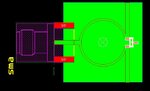
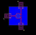
How to fix this design rule problem in Altium. Why I have problems while connecting signal pin to microstrip. And should i send ground pin footprint on bottom layer. Any Suggestions? attached is a picture. Sorry for such a basic Question.
Capture.JPG
 

Obviously, the top ground pins must not short the coupler traces and should have some distance to it not to disturb their impedance too much. So the PCB size should be adjusted, or you need to cut the pins manually.

Usually you have pads for the top ground pins, connected to the ground plane by multiple vias in case of a microstrip.
 

I want to connect ground pins of sma to bottom ground plane is that ok to shift to bottom layer???and signal pin and coupler are on top layer. when i place signal pin on couple it becomes short. how to solve this issue. top layer does not have any ground plane.i can extend the size.No issues.
 

Attachments

  • Capture.JPG
    Capture.JPG
    46.3 KB · Views: 142

Use a different connector (flange type). Your design will not work well.
 

Volker please share your reasons also if you can comment on my doubts. actually i need feeding circuit made of some couplers to feed antenna on other side. So i can't place connector on other side.
Regards
 

Most of my concerns may be solved by assigning names to the nets. But I am not sure how to name in PCB file. Also i am not sure if it is standard procedures for RF PCB design. I have never send pcb to manufacturer till now. I hope many of the people on this forum has gone through these steps many times. I hope from you guys to explain to me on very basic level. I am sure these are very minor issues. I am posting this because none of the forum satisfy me this regards and also I don't have such expertise in my surroundings. I will be very thankful for this.
PS: My frequency of operation is 3.5 GHz.
 

Use a different connector (flange type).
Nothing has been said yet about a case where a flange could be mounted.

Edge mounted SMA gives best RF performance for a bare PCB. As said, it would be better to connect the top ground pins, but without it, connector VSWR can be still acceptable. If you have a throughplated PCB, I don't see why you won't place top ground pads with vias.

Sufficient distance of the ground pins respectively pads to the coupler structure is required anyway.
 
Why circuit turn to green. how to solve this issue?
For top ground pads i can add vias with a distance less than quarter wavelength longer line for better VSWR. No issue.
Help me taking a step from theory to practical design.

Best Regards,
Rizwan
 

You can see the error(s) by right clicking the green place, there should be "Violations" in the right click menu. You can also run DRC(design rule checker under Tools menu) to see errors. Design rule errors can be fixed or they may not be important. You should be careful about whether there is a mistake in your design.
 
Thank You guys for your valuable suggestions. My only problem was software understandings. Any ways your valuable suggestions are alot helpful too me. Now I get things as here
 

Attachments

  • Capture.JPG
    Capture.JPG
    22.6 KB · Views: 122

Status
Not open for further replies.

Part and Inventory Search

Welcome to EDABoard.com

Sponsor

Back
Top