Continue to Site

Welcome to EDAboard.com

Welcome to our site! EDAboard.com is an international Electronics Discussion Forum focused on EDA software, circuits, schematics, books, theory, papers, asic, pld, 8051, DSP, Network, RF, Analog Design, PCB, Service Manuals... and a whole lot more! To participate you need to register. Registration is free. Click here to register now.

[SOLVED] 7 Segment 5 Digit Driver

Status
Not open for further replies.

actor23

Member level 3
Joined
Dec 12, 2014
Messages
56
Helped
1
Reputation
2
Reaction score
1
Trophy points
8
Activity points
515
Hello All ;

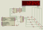
I've been working the circuit schematic of 5 digit 7 segment leds.

My ICs and discrete elements are :

TPIC6b595 (Shift Register)
CD4017 (Decade Counter)
5xNpn BJT
5 Digit Common Anode Led Display
5 Buttons directly connect to uC

My question about coding. Shift register' inputs driven by uC deciding by the buttons. Which are set,up,down,shift,mode,etc. I am planning to use 25Hz-50Hz clock signal to feed the CD4017 which is used for selecting the digits. In the timer interrupt vector, should i update the data on the each digit ? Or, how i can do this ? When a button is pressed an interrupt is created should it be updated in the interrupt vector by writing value in an array ?

Im sending a bit messy schematic for you,it is hand drawing. Hope one who did this before want to help me.

Thanks in advance.

Best Regards
20150916_151423.jpg
 

As you are using only one TPI6b595 and multiplexing the 5 digits then you need to update the data of TPIC6b595 say once every 2 ms. For example you have 5 digits and there will be 5 different data for the five digits and so you write each data for TPIC6b595 and after 2 ms you write new data. For this you have to use 2 ms Timer interrupt.

When a button is pressed an interrupt is created should it be updated in the interrupt vector by writing value in an array ?

What do you mean by this ? Do you want to increment or decrement the value displayed on the 7 Segments using buttons ? If yes, then you have to split the number to digits and then convert them to their respective 7 Segment masks and then send one mask to 595 and then turn on that digit for 2 ms and then turn OFF that digit and then send data of next digit and turn ON the second digit and repeat the process for all the digits.

I am not sure whether the NPN transistors will do the job or not because to drive a Common Anode 7 Segment display you need a PNP transistor.
 
Last edited:

Thank you for reply pic.programmer ;

Firstly, yes buttons will increment and decrement the values of each digit. Also, one button blink the selected digit which will be changed. Eventually, set button write determined value to digit and blinking cancelled. My question was that when this mask value should be changed ? In the interrupt service routine of timer or buttons interrupt service routines ?

CD4017 generates clock pulse given frequency for first output,then generates the same pulse after 9 period are completed. So, when its 5 outputs connects the Led's common modes, is 1 digit flashes for 1 period of clock signal,after it flashes 9x(1 period of clock signal) ? Also, when CD4017 output signal goes high it is connected to npn base. So, it causes bjt to open then common anode tied to +5V which is the voltage of collector ?
 

When you want to display 25 then you have to send mask of 5 and then turn on digit one (units digit) then it will be ON for 2 ms and then you turn OFF digit one and then you send mask for 2 and then turn on tens digit and keep it ON for 2 ms and then repeat the cycle. You need only one Timer Interrupt to do this. For buttons you can use ordinary non interrupt buttons. To blink a digit like say you want to blink 5 then you have to use a counter which will hold the time for which display will be ON and then toggle a flag and count same time again with displays OFF. This will give blinking effect when you are setting a value.

Only one output of CD4017 will be high at a time and after 5th pin oes high and turns ON digit 5 and then turns OFF then you can reset Cd4017 and start another cycle of data writing.

Yes, as you have connected emitter to common anode pins your circuit will work. I tested your setup in Proteus and it works.

Which microcontroller do you want to use to drive the 595 and 4017 chips ?

Do you want to display integer value or floating point value ?

Do you want to display leading zeroes like in 00452 or do you want to block them and display as 452 ?
 
Last edited:

Bro, thank you for this answer. I am considering about working principle of the TPIC6b595. Does it works unsyncronized ? So, when user gives any input by using buttons. It changes the state of the led. Let me give an example of what i will do ; For example ;

Code:
#pragma vector=VECT_MTU0_TCOV4     //overflow 
_interrupt void CD4017_CLK(void)          // repeat every 2 ms f.e
{
mc_delay(100);                                    //wait 100ns for rise time of CD4017
count++;                                            //which is 0 above the routine

if(count==1){ led_write(5); }               //first digit value--- led_write(); changes the GPIO pins of TPIC6b595

if(count==2){ led_write(2); }              //second digit value 
-
--
----
---
--

if(count == 6){count = 0; }
etc..

Here is the quick example
I change the TPIC6b595 in the service routine when the second overflow comes. Every interrupt comes 500Hz. One digit off time is equal 5x1/500Hz = 10ms so it does not blink while normal operating actually human eye cannot realize the off time. So is it like that or any code suggestions ?

Also could you send me the proteus of this circuit if you simulate it all ?
 
Last edited by a moderator:

Before answering I have to write a small piece of code and see if it works because now I have a doubt that it will not work because you cannot turn OFF output of 4017. One output pin of 4017 will be ON at a time and if you shift new data to 595 then it will be displayed in wrong digit position as you don't have option to turn OFF 4017 outputs. I will see if it works like this

Send mask of digit 1 to 595 and send one clock to 4017 then after 2 ms turn OFF 4017 and then send mask of digit 2 to 595 and then give two clocks to 4017 and turn it ON. I have to see if this method works. Give me two hours. I will write a code and see if this logic works.

Instead of 4017 and NPN transistors if you use 74LS145 and PNP transistors then it works.

- - - Updated - - -

I found a way to make it work. You have to do as shown in the below algorithm. Q0 of 4017 is not used. Q1 to Q5 are used for the 5 digits. You didn't mention which microcontroller you want to use. Anyways, it can be implemented.

Code:
char mask[10] = {0 to 9};
char select = 0;


void sendByte(unsigned char byte) {

	char i = 0, mask = 0x80;

	for(i = 0; i < 8; i++) {
		if(byte & mask) {
			DS = 1;
		}
		else {
			DS = 0;
		}	

		SH_CP = 1;
		Delay_us(500);
		SH_CP = 0;

		mask >>= 1;
	}

	ST_CP = 1;
	Delay_us(500);
	ST_CP = 0;
}

void ISR() {

	switch(select) {

		case 0:
			sendByte(mask[a]);
			4017_CLK = 1;
			Delay_us(200);
			4017_CLK = 0;
			break;			
		case 1:
			sendByte(0xFF);
			4017_CLK = 1;
			Delay_us(200);
			4017_CLK = 0;
			break;	
		case 2:
			sendByte(mask[b]);
		case 3:
			sendByte(0xFF);
			4017_CLK = 1;
			Delay_us(200);
			4017_CLK = 0;
			break;	
		case 4:
			sendByte(mask[c]);
		case 5:
			sendByte(0xFF);
			4017_CLK = 1;
			Delay_us(200);
			4017_CLK = 0;
			break;	
		case 6:
			sendByte(mask[d]);
		case 7:
			sendByte(0xFF);
			4017_CLK = 1;
			Delay_us(200);
			4017_CLK = 0;
			break;	
		case 8:
			sendByte(mask[a]);
		case 9:
			sendByte(0xFF);
			RESET 4017

	}

	if(++select == 10)select = 0;

}
 

Before answering I have to write a small piece of code and see if it works because now I have a doubt that it will not work because you cannot turn OFF output of 4017. One output pin of 4017 will be ON at a time and if you shift new data to 595 then it will be displayed in wrong digit position as you don't have option to turn OFF 4017 outputs.

There is one possible way to blank the display between digits. The 4017 has 10 outputs, and if you connect every second output to a digit, that is output 1,3,5,7,9 to the digits, you can blank the digit between each digit and at reset.

This makes it possible to reduce the ghosting between digits.

Another thing is the common anode drivers. You need a base resistor for each transistor. From the drawing it looks like these are crossed out. If you don't use resistors, the transistors Vbe will short the output to Vcc-0.7V when it is pulling low.
 

Here I made a sample code using PIC microcontroller but I think you are not using PIC microcontroller but the logic of working is same. You have to create a 2 ms timer interrupt and send the data. I am working on code to blink a selected digit when in set mode. I will soon post the code which includes blinking of digit. Here I am attaching a project with Proteus 8.2 SP2 format file. If you have proteus then you can test the simulation or if you don't have then see the attached image. The project is written using mikroC PRO PIC Compiler because that is the Compiler I use most often but if you are using ARM microcontroller then I can write a code for ARM microcontroller also.
 

Attachments

  • SSD.rar
    27.2 KB · Views: 159
  • ssd.png
    ssd.png
    79.9 KB · Views: 634
  • Like
Reactions: actor23

    actor23

    Points: 2
    Helpful Answer Positive Rating
Great helping and great explanations thank you all !

Gorgon, your idea is smart i will try. Also, the schematic which i've drawn is not correct at all. For instance, i will put resistor on the anode of each digit. I think it blocks the unwanted current spikes also excess current. Why bjt short out i don't understand ? When Vbe reaches +0.7V switch will be on state then anode connects to +5V ?

pic.programmer, bro in timer interrupt you don't give pwm output to 4017 clk. Hmm, i've analyzing your last circuit which is in proteus. Also, my microprocessors are either renesas rx62t or msp432p... series.
 

Hi I have IAR RX Compiler for Reneasas RX microcontrollers but have not used it much. The logic is simple. You need to create a 2 ms Timer Interrupt and do the code inside switch statement (in ISR). To create blinking and shift effects you need another timer and you have to create a timer interrupt of 500 ms and use it.

See attached videos. (mods I uploaded the video to youtube but the quality after uploading was very poor (blur)). Hence I am attaching simulation video here. It is compressed and it is only 284 KB. If you think the file is big then you can delete it.

@actor

See attached video. Do you want something like these ?
 

Attachments

  • sim videos.rar
    283.7 KB · Views: 122
  • Like
Reactions: actor23

    actor23

    Points: 2
    Helpful Answer Positive Rating
I' ve just watched your videos thanks for all.But if i ask for detailed explanation of the code ? For example, what is
if(TMR1IF_bit) {
TMR1H = 0xF8;
TMR1L = 0x30;

this part ? This is related to timer you used ? Also ;
display[0] = mask[number / 10000];
display[1] = mask[(number / 1000) % 10];
This part in the while(); what indicates ?

Lastly, could you please tell me the last project which includes blinking in the video ? Also, what does DS variable mean ?

Oops you used another level shifter ic 74HC595 is it same characteristic with TPIC ? Sorry, but confused about the shifter pins coding :?:
 

This piece of code is the timer1 interrupt code

Code:
if(TMR1IF_bit) {
TMR1H = 0xF8;
TMR1L = 0x30;

You don't have to worry about it as you are using Reneasas microcontroller. Just create a Timer Initialization function which Initializes Timer X to create 2 ms Timer interrupt. Then create ISR for the Timer Interrupt and then copy and paste the switch statement.

In the above code it is checking if Timer 1 Interrupt Flag is set and then if Timer 1 Interrupt flag is set then it is reloading the Timer variable with the preload value so that it can count for the next timer interrupt.

In the below code

Code:
display[0] = mask[number / 10000];
display[1] = mask[(number / 1000) % 10];
I am splitting the number into digits and then taking the respective masks for the digits so that it can be set to 595. There is no TPIC in Proteus and hence I have used HC595 but I am sure TPIC IC will be same as 74HC595 as they both are 8 bit shift registers.

I will soon post the code for blinking and shifting displays.
 

Gorgon, your idea is smart i will try. Also, the schematic which i've drawn is not correct at all. For instance, i will put resistor on the anode of each digit. I think it blocks the unwanted current spikes also excess current. Why bjt short out i don't understand ? When Vbe reaches +0.7V switch will be on state then anode connects to +5V ?

I stand corrected, I saw the transistors as PNP, but they are NPN. You are correct, you really don't need base resistors. The 4017 output will, drive to almost 5V, and the emitter of the transisor will be at 4.3V. This way you loose 0.7V over the transistor, and will burn some power over it too. But it should work.

Just had a look at the tpic6b595 datasheet, if you need inter digit blanking, you can also use the /G input to disable the outputs, if you have an output extra available.
 
Last edited:

I checked the datasheet of the TPIC device (tpic6b595). It is same as 74HC595 except it can drive larger load.

The (G Bar) pin of TPIC is equal to OE Bar pin of 74HC579.
The (SRCLR Bar) pin of TPIC is equal to MR Bar pin of 74HC595.
SER IN pin is equal to DS pin
SRCK pin is equal to SH_CP (shift clock pulse)
RCK is equal to ST_CP (storage clock pulse)

Here I am attaching code for blinking selected digit and also for scrolling display. I can write a better code for scrolling display using pointers. If you are interested then I will write a code for you using pointers but not for your micrcocontroller but for PIC to show you how to make it using pointers.

You make a template code which contains a Timer X Initialization function which initializes the Timer X to 2 ms interrupt and an ISR routine which tests if Timer Flag was set and reloads the timer register for your Reneasas microcontroller. I will add the 7 Segment Driving code to it.

The outputs of TPIC6b595 are open drain outputs and hence you will need 8 pull up resistors at the outputs of it.
 

Attachments

  • SSD blinking code.rar
    30.1 KB · Views: 174
  • SSD shifted display.rar
    32.9 KB · Views: 130
Last edited:
  • Like
Reactions: actor23

    actor23

    Points: 2
    Helpful Answer Positive Rating
What's all this stuff about Ohm's Law , duty cycle and loss of efficacy for small duty cycles with high Ipk/Iavg?


Whenever you MUX LEDs you are limited on the duty cycle because the Absolute Max mA/ Rated mA is often only 3. Therefore increase the duty cycle from 5 to 10 makes the average current much lower than rated and thus much dimmer. or limited to 60mA /10 = 6mA average or 6mA/20mA=30% of rated intensity.
Bad idea.

A typical 10mm 7seg LED is rated for 20mA continuous and 60mA MAX
So using a 5 Digit MUX means you can only drive the LED at 12mA average at 20% duty cycle.
Using 500Hz fram rate will not produce any flicker and 2.5kHz digit clock increment rate should not produce much blurring.

However using a Common Anode series resistor is a bad idea since the voltage drop and thus intensity will reduce according tot he number of segments active. So using 60mA max at 20% d.f. * 7 segments or 300mA per digit must be at a constant voltage. Since the 4017 has a low drive current with <10% drop of-0.51mA min and -1mA typ at 25'C with 4.6V out from Vcc=5V you need a current gain in the NPN anode drivers of 300mA/0.5mA or 600x. THis can only be obtained with a Darlington. Now it is smarter to use Common Cathode with ULN200x Darlingtons x 7.. oh well.

Next you need to use Ohm's Law on the voltage drop.
4017 =0.4V @0.5mA @ Vcc=5V at 25'C
Darlington e.g. MMBT6427 for 300mA Vbe=1.25V @ 25'C at Ie=60mA
7 seg Red Vf=2.3V @ 60mA
Segment driver = 5.5Ω * 60mA = 330mV
Segment R series =?
Thus assuming V+=5V total drop is 0.4V +1.25+2.3V+0.33=4.28V leaving 0.72V to draw 60mA per segment.
This means the Rseries is 0.72V/60mA= 12Ω ( not 330Ω)
A tolerance analysis on each variable will increase Rseries to a safe value so as not to exceed 60mA max per segment.
e.g. if +5V is 5% or 5.25V then R series is 16Ω

To prevent bleeding between digits. each digit driver must be turned off fast.Thus a dummy load of 10% can be tolerated or 30mA@ (5-0.4-1.25V=3.35V/30mA=111Ω or 120Ω across Anode to ground.
Cebo is roughly 10~20pF when driver is reverse biased , Cibo is 15pF.
Using a 1 segment being tuned off the load ESR is ~10Ω thus 20pF*10Ω=peanuts for the driver.
LED decay time is fast at 500Hz Display frame rate.
 

Study the attached code. It is very easy to port the code to any microcontroller. I have simplified the ISR code using pointer. This is a new version of code for static 7 Segment Display using pointer.
 

Attachments

  • SSD Using Pointer.rar
    27.8 KB · Views: 142

@pic.programmer

Code:
 if((select == 0) || (select == 1) || (select == 3) || (select == 5) || (select == 7) || (select == 9)) {
                   CD4017_CLK = 1;
                   Delay_us(200);
                   CD4017_CLK = 0;

At first time when interrupt occurs so, select = 0 and sendByte sends data to shift register. After 4ms when select =3 CD4017 clock goes high but, in the above case 3,5,7,9 sendByte(0xFF) so disable all outputs of the LED when CD4017 clock high also outputs are enabled. Is this process done when the select =0,2,4,6 ? Confused :(
 

Code:
char mask[10] = {0xC0, 0xF9, 0xA4, 0xB0, 0x99, 0x92, 0x82, 0xF8, 0x80, 0x90};
char select = 0;
unsigned int number = 12345;
char display[5] = {0xFF, 0xFF, 0xFF, 0xFF, 0xFF};

char *ptr2char = 0;

sbit SH_CP at LATC0_bit;
sbit DS at LATC1_bit;
sbit ST_CP at LATC2_bit;

sbit CD4017_CLK at LATC3_bit;
sbit CD4017_RST at LATC4_bit;

//Timer1
//Prescaler 1:1; TMR1 Preload = 63536; Actual Interrupt Time : 2 ms
//Place/Copy this part in declaration section
void InitTimer1() {
    T1CON = 0x01;
    TMR1IF_bit = 0;
    TMR1H = 0xF8;
    TMR1L = 0x30;
    TMR1IE_bit = 1;
    INTCON = 0xC0;
}

void sendByte(unsigned char byte) {
    char i = 0, mask = 0x80;

    for(i = 0; i < 8; i++) {
            if(byte & mask)
                DS = 1;
            else
                DS = 0;

            SH_CP = 1;
            Delay_us(50);
            SH_CP = 0;

            mask >>= 1;
    }

    ST_CP = 1;
    Delay_us(50);
    ST_CP = 0;
}

void Interrupt() {
    if(TMR1IF_bit) {
        //Enter your code here
        TMR1H = 0xF8;
        TMR1L = 0x30;
        switch(select) {
                case 0:
                case 2:
                case 4:
                case 6:
                case 8:
                     sendByte(*ptr2char++);
                     break;
                case 1:
                case 3:
                case 5:
                case 7:
                case 9:
                      sendByte(0xFF);
                      break;
        };

        ++select;

        if((select == 0) || (select == 1) || (select == 3) || (select == 5) || (select == 7) || (select == 9)) {
                   CD4017_CLK = 1;
                   Delay_us(200);
                   CD4017_CLK = 0;
        }

        if(select == 10) {
              CD4017_RST = 1;
              Delay_us(200);
              CD4017_RST = 0;
              select = 0;
              ptr2char = &display;
        }


        TMR1IF_bit = 0;
    }
}

void main() {

     CM1CON0 = 0x00;
     CM2CON0 = 0x00;
     
     SLRCON = 0x00;
     
     ANSELA = 0x00;
     ANSELB = 0x00;
     ANSELC = 0x00;
     
     TRISA = 0xC0;
     TRISB = 0x03;
     TRISC = 0x00;
     
     PORTA = 0x00;
     PORTB = 0x00;
     PORTC = 0x00;
     
     LATA = 0x00;
     LATB = 0x00;
     LATC = 0x00;
     
     ptr2char = &display;
     
     InitTimer1();
     
     while(1) {
          display[0] = mask[number / 10000];
          display[1] = mask[(number / 1000) % 10];
          display[2] = mask[(number / 100) % 10];
          display[3] = mask[(number / 10) % 10];
          display[4] = mask[(number / 1) % 10];
     }
}


//This is how it works.

Code:
display[0] = mask[number / 10000];
display[1] = mask[(number / 1000) % 10];
display[2] = mask[(number / 100) % 10];
display[3] = mask[(number / 10) % 10];
display[4] = mask[(number / 1) % 10];

if number is 12345 then

number / 10000 = 1 (integer value)

mask[] contains the 10 masks for 7 segment display for common anode display.

mask[0] = 0xC0 will display 0 on the 7 segment.

here result is 1 and so

display[0] = mask[1] which will display 1 on the 7 Segment

Similarly

number / 1000 will give 12 and mod (%) of 12 is 2 and display[1] = mask[2] will display 2 on 7 Segment

Similarly other digits of the number (here 12345) are extracted and converted to their respective 7 Segment mask
and filled in display[] array used for displaying

then mask = 0x80 used in the sendByte() function is different from the global array mask[].
Code:
//Timer1
//Prescaler 1:1; TMR1 Preload = 63536; Actual Interrupt Time : 2 ms
//Place/Copy this part in declaration section
void InitTimer1() {
    T1CON = 0x01;
    TMR1IF_bit = 0;
    TMR1H = 0xF8;
    TMR1L = 0x30;
    TMR1IE_bit = 1;
    INTCON = 0xC0;
}
The above InitTimer1() function when called (here once) initializes the Timer to 2 ms interrupt and so the ISR is called once every 2 ms.

Code:
void sendByte(unsigned char byte) {
    char i = 0, mask = 0x80;

    for(i = 0; i < 8; i++) {
            if(byte & mask)
                DS = 1;
            else
                DS = 0;

            SH_CP = 1;
            Delay_us(50);
            SH_CP = 0;

            mask >>= 1;
    }

    ST_CP = 1;
    Delay_us(50);
    ST_CP = 0;
}
sendByte() is the core function used to send byte (here mask[] values stored is display[]) to TPIC6b595 (HC595).

the for() loop loops 8 times (0 to 7) and in each loop the byte is anded with mask (here 0x80 as starting value) and if the result is true then
1 is placed on DS (pin connected to DS of TPIC, Data Serial), if result is 0 a 0 is placed on the DS pin and then a Shift clock pulse (SH_CP) is
provided to shift in the bit (0 or 1) into DS (shift register). Then mask>>= 1 will shift the value 0x80 to 0x40 and then in the next loop when this
0x40 is used to and with byte then bit 6 (bits 0 to 7) of byte is tested for 0 or 1. Them mask>>= 1 will make the mask value 0x20, then 0x10,
0x08, 0x04, 0x02, and finally in the 8th loop 0x01 and anded with byte (which contains the mask[] value stored in display[x] or the mask value
pointed to by the pointer *ptr2display.

finally when 8 bits of data are shifted to shift register with eight SH_CP then one ST_CP (storage clock pulse) is provided to make the mask value
contained in display[x] to appear at the output of the TPIC.

a pointer (ptr2display) is used to send the value in display[x] to the sendByte() function.

display[5] is a 5 element array with elements 0 to 4. The start address of display[] which is also the address of display[0] is assigned to
the pointer ptr2display and this is incremented with *ptr2display++ in the switch statement when the value of select variable is 0, 2, 4, 6, 8

The timer value is loaded on each interrupt to Timer register using
Code:
TMR1H = 0xF8;
TMR1L = 0x30;
so that Timer can count another 2 ms for the next timer interrupt.


In this code
Code:
sbit SH_CP at LATC0_bit;
sbit DS at LATC1_bit;
sbit ST_CP at LATC2_bit;

sbit CD4017_CLK at LATC3_bit;
sbit CD4017_RST at LATC4_bit;
SH_CP is the pin RC0 of PIC microcontroller
similarly other pins. LATxy is the output register of PIC. LATC0_bit is the bit 0 of the LATC regisater used to output 1 or 0. It is the digital
IO pin.


Here is how the ISR works. It is called once every 2 ms.

Code:
switch(select) {
                case 0:
                case 2:
                case 4:
                case 6:
                case 8:
                     sendByte(*ptr2char++);
                     break;
                case 1:
                case 3:
                case 5:
                case 7:
                case 9:
                      sendByte(0xFF);
                      break;
        };

        ++select;

        if((select == 0) || (select == 1) || (select == 3) || (select == 5) || (select == 7) || (select == 9)) {
                   CD4017_CLK = 1;
                   Delay_us(200);
                   CD4017_CLK = 0;
        }

        if(select == 10) {
              CD4017_RST = 1;
              Delay_us(200);
              CD4017_RST = 0;
              select = 0;
              ptr2char = &display;
        }

when select is 0 (display[0] which is pointed to by the pointer *ptr2display is send to TPIC and then

Code:
if((select == 0) || (select == 1) || (select == 3) || (select == 5) || (select == 7) || (select == 9)) {
                   CD4017_CLK = 1;
                   Delay_us(200);
                   CD4017_CLK = 0;
        }

will give a clock to CD4017 and make its second pin high which will turn on the ten thousandth digit of the 5 digits.

Next when select is , 0xFF is sent to TPIC to turn OFF the 7 Segment so that the CD4017 output can be shifted. Then as select is 1
the above if() condition again sends a clock to CD4017 and the (Q2 pin of Q0 to Q9) will become high but as 0xFF is placed at output of TPIC the 7 segements will be OFF.
Then when select is 2 (display[1] pointed to by pointer *ptr2display++ (incremeted pointer)) is placed at output of TPIC and as thousandth digit is already
ON the digit (2 here) is displayed on thousandth place.

when select is 10, CD4017 is reset and its Q0 pin becomes high which is not connected to any display. select is reset to 0 and pointer is also reset so that it
again points to display[0].

As you said you tested my Proteus file I assume you have Proteus. If you have then load my .cof file for the simple static display and debug it step by step and see what happens.
 
  • Like
Reactions: actor23

    actor23

    Points: 2
    Helpful Answer Positive Rating
when select is 0 (display[0] which is pointed to by the pointer *ptr2display is send to TPIC and then will give a clock to CD4017 and make its second pin ......

at first, Q0 is high ? So, when first interrupt comes (select = 0) Q1 is on firstly not Q0 which is not connected anywhere ?? If then, everything is okey. Also, thanks for this amazing explanation bro.

Actually, i will explain you what i want to via mail.
 

See the circuit in post #8. Q0 of CD4017 will be high initially and hence left unconnected. When select is 0 display[0] value is placed at output of TPIC and a clock is given to CD4017 and this makes Q1 of CD4017 go high which will turn on ten thousandth place digit which will display 1 of the number 12345. Then 2 ms nothing happens. Then on second interrupt select will be 1 and hence 0xFF is sent to TPIC and the ten thousandth place digit is turned OFF and then clock is given to CD4017 and Q2 of CD4017 becomes high and it turns tousandth place digit but as TPIC outputs are 0xFF nothing appears. Then after 2 ms and when select is 2, display[1] data is sent to TPIC and as Q2 is already high the thousandth place digit will display 2 of 12345.
 

Status
Not open for further replies.

Similar threads

Part and Inventory Search

Welcome to EDABoard.com

Sponsor

Back
Top