dany.1986
Junior Member level 1
Hi
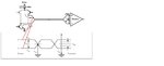
I have a problem understanding how a differential signalling works. I have combined two most common graphical explanations about differential signalling into the attached picture. My questions are:
Do V+ and V- correspond to the nets pointed in the picture by the red arrows?
If VOD is 0.350 V max, and VOS is 0.7 V min and 1.2 V max then is it correct to calculate VOH and VOL as follows:
VOH= VOS max + |1/2*VOD max| so VOH= 1.2 + |1/2*0.350|= 1.325 V ???
VOL= VOS min - |1/2*VOD max| so VOL= 0.7 - |1/2*0.350|= 0.575 V ???
In the current configuration (the one in the top of the picture) the receiver sees that V+ is 1.325 V and V- is 0.575 V and interprets it as logic '1' ???
If the mosfets referenced by the negative sign are closed then does it mean that V + becomes 0.575 V and V- becomes 1.325 V so that the receiver will interpret it as logic '0' ???