Continue to Site

Welcome to EDAboard.com

Welcome to our site! EDAboard.com is an international Electronics Discussion Forum focused on EDA software, circuits, schematics, books, theory, papers, asic, pld, 8051, DSP, Network, RF, Analog Design, PCB, Service Manuals... and a whole lot more! To participate you need to register. Registration is free. Click here to register now.

[SOLVED] Flash timing waveform for Write buffer programming

Status
Not open for further replies.

rahdirs

Advanced Member level 1
Joined
May 22, 2013
Messages
424
Helped
93
Reputation
192
Reaction score
91
Trophy points
1,308
Location
Mordor
Activity points
4,492
Hi,

I'm trying to write a flash controller for writing,reading etc... into NOR flash S29GL01GP.
I have implemented the cycles that i need to follow for Program,Buffer Program,Erase etc.. as per the data sheet.Only thing left is to assert CE,OE,WE for the cycles based on the timing diagram given in the data sheet.

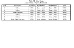
Example: To do buffer programming i have to follow the following cycles:
Buffer_Prog.JPG

After writing an fsm which follows the above cycles,i need to following the timing diagram to drive CE,WE,OE etc....But i can't find the timing diagram for Buffer write programming.I can only fing timing diagram for Single Word Programming which is:
timing_diagram.JPG

So how do i drive CE,WE,OE for the buffer programming ?

Datasheet: www.spansion.com/Support/Datasheets/S29GL-P_00.pdf
 

The timing waveforms are the same look at the timing specification for tWHWH1. Table 11.6 S29GL-P Erase and Program Operations on pg 61 and pay attention to Note 4.
Capture.JPG

FYI RY/BY# controls when you know the program operation is complete, so the buffer writes use a shorter interval for tWHWH1 probably the last write to the buffer that then gets programmed into the nor array will take the full "Write Buffer Program Operation" time.
 
  • Like
Reactions: rahdirs

    rahdirs

    Points: 2
    Helpful Answer Positive Rating
@ads-ee:

In the timing waveform for program command (4 cycle command) attached in post #1,he shows the timing sequence for only last 2 cycles and for the rest of the cycles it is don't care?

From argument by @ads-ee in post#2 i think both program & buffer write have the same timing cycle.

Based on the number of data words you are writing in a single go,the number of cycles can be from 6(1 data word at a time) to 37(32 data words at a time) at maximum.

So if you are buffer writing 32 words at a time,for which two cycles should i follow that timing diagram? 36 to 37 or 5 to 6 ?
 
Last edited:

Saying the timing diagram in post #1 is a "4 cycle command" misses the point. Instead it shows different phases involved with programming:
- issuing the 0xA0 program command
- write program data
- polling for programming completion

The same phases occur in multi byte ("buffer write") programming, but the data phase is repeated. There's no specific timing to be observed, besides that you need to keep the requirements for write and read cycles regarding setup and hold times and minimal pulse widths.
 

Saying the timing diagram in post #1 is a "4 cycle command" misses the point. Instead it shows different phases involved with programming:
For a single word programming,this is the command cycle to be followed:

Program.JPG

So,for example the toggling of CE signal is only at the last two command cycles & at the rest of the command sequence i can keep CE as '0' or '1'?
broken link removed
 
Last edited by a moderator:

So,for example the toggling of CE signal is only at the last two command cycles & the rest i can keep CE as '0' ?
Yes.

Additionally, in many cases, a CE change in the timing diagrams doesn't mean that CE must be actually operated. It only shows the required relation between CE and the second control signal, OE or WE.
 

@FvM:

Similarly for the write buffer command(with 32 data words) it is enough if i toggle CE & follow those setup,hold times for cycle no. 4 & data cycle which keeps on repeating for cycle 5 to 36; the rest all are don't care ?
broken link removed
 
Last edited by a moderator:

Yes.

Additionally, in many cases, a CE change in the timing diagrams doesn't mean that CE must be actually operated. It only shows the required relation between CE and the second control signal, OE or WE.

or if i just follow the toggling of CE & corresponding sequence of WE & OE as shown in timing diagram of post #5 at each cycle during the entire write buffer programming,it should be fine ?
 

Issue with NOR Flash Operations from FPGA

Hi,

I am trying to store my fpga design data into a NOR flash(S29GL01GP).For that i've written a flash controller code as per the data sheet.

To check if my code works properly,i'm writing a counter into the flash.

The way i'm testing flash:- As of now,i'm only doing Single word programming.I have a UART connected,so from UART if i give write command 5 times it writes at addr 0,1,2,3,4 data 0,1,2,3,4 respectively.Similarly if i give write command 10 times at addr 0..9 it writes data 0...9

My problem: After writing an x number of times,i'm reading 1024 address locations starting from 0 to 1023.I'm only reading back the last data that i've wriiten.
Suppose,i have given write command 3 times at addr 0..2,data 0..2 is written.So while reading 1k addresses i'm only reading data value '2'(the last written data.If i write x times,i read only x).

What could be the issue ?
 
Last edited by a moderator:

Do you wait for finish of each write command before starting a new one?
 

Do you wait for finish of each write command before starting a new one?

According to datasheet,Single word programming takes 60 us,so conservatively i can say the operation completes in 100 us.

But anyway as i already said i'm giving the write command by using UART from PC,it must be at least a gap of 5 s between two write commands.
 

O.k., enough time for the write operation to fnish.

Of course we don't know what you are exactly doing. How and when are you erasing the flash sector? Which value do you read from the other locations?
 

Of course we don't know what you are exactly doing. How and when are you erasing the flash sector? Which value do you read from the other locations?

As of now,i'm only performing operations only in sector 0.After applying reset,i'm doing sector 0 erase & after that i'm giving write commands starting from addr 0;then i'm reading 1k addr locations from 0 to 1023.

What do you mean how are you erasing the flash sector --- ?

As i'm doing operations only on sector 0,i'm doing only sector 0 erase as per data sheet attached.

Which value do you read from the other locations?

Say,i write 3 address locations with data values 1,2,3 & as i'm trying to read 1k locations from 0 to 1023 at addr 0,1,2 i should read 1,2,3 & all other addresses from 4 to 1023 i should read FFFF(because after sector erase i did not write anything to those locations).
But i'm reading at all the other addresses including 0,1,2 is the last address data value which i have written(in the above example 3) .
 

Attachments

  • untitled.JPG
    untitled.JPG
    57.4 KB · Views: 110

Looks like either the write or the read sequence isn't performed as intended (respectively required).

Did you check the design in a simulation?
 

Looks like either the write or the read sequence isn't performed as intended (respectively required).
Did you check the design in a simulation?

I did not check with the flash model file,i was getting compilation issues with it,but i checked my fsm's in simulation to see what sequence they are writing to flash.

From the below two simulations,we can know the sequence followed
Write:-

write.JPG

read:-

read.JPG
 

Looks like either the write or the read sequence isn't performed as intended (respectively required).

Did you check the design in a simulation?

@Fvm:

I finally completed simulating my design with flash model file,
the earlier issue of read data being last written data had to be with me not assigning the flash_data which is an inout port through a tristate buffer.

Now that is done,after doing a sector erase & writing to 10 addresses & then reading i can see that data is not written at those addresses.So this could mean that my write sequence is wrong.

My write sequence code:-
output process snippet

Code VHDL - [expand]
1
2
3
4
5
6
7
8
9
10
11
12
13
14
15
16
17
18
19
20
21
22
23
24
25
26
27
28
29
30
31
32
33
34
35
36
37
38
39
40
41
42
43
44
45
46
47
48
49
50
51
52
53
54
55
56
57
58
59
60
61
62
63
64
65
66
67
68
69
70
71
72
73
74
75
76
77
78
79
80
81
82
83
84
85
86
87
88
89
90
91
92
93
94
95
96
97
98
99
100
101
102
103
104
105
106
107
108
109
110
111
112
113
114
115
116
117
118
119
120
121
122
123
124
125
126
127
128
129
130
131
132
133
134
135
136
137
138
139
140
when data_write_1_1 =>          
                USERFL_CEn1     <= '1';
                USERFL_OEn      <= '1';
                USERFL_WEn      <= '1';
                dsel <= x"1";      --- data = x"00AA"
                asel <= x"1";      ---   address =  x"0000555"
                msel <= '1';
                writeo <= '0';
                testo <= x"02";
                b <= x"0000";
                a <= x"0";
                wait_cnt <= x"0000";
            when data_write_1_2 =>          
                USERFL_CEn1     <= '0';
                USERFL_OEn      <= '1';
                USERFL_WEn      <= '1';
                writeo <= '1';
                a <= a + '1';
                testo <= x"03";
            when data_write_1_3 =>          
                USERFL_CEn1     <= '0';
                USERFL_OEn      <= '1';
                if (b <= 8) then
                USERFL_WEn      <= '0';
                else
                USERFL_WEn      <= '1';
                end if; 
                writeo <= '0';
                a <= x"0";
                testo <= x"04";
                b <= b + '1';
            when data_write_2_1 =>          
                USERFL_CEn1     <= '1';
                USERFL_OEn      <= '1';
                USERFL_WEn      <= '1';
                dsel <= x"2";        -- data = x"0055"
                asel <= x"2";           -- address = x"00002AA"
                msel <= '1';
                writeo <= '0';
                testo <= x"05";
                b <= x"0000";
                
            when data_write_2_2 =>          
                USERFL_CEn1     <= '0';
                USERFL_OEn      <= '1';
                USERFL_WEn      <= '1';
                writeo <= '1';
                a <= a + '1';
                testo <= x"06";
            
            when data_write_2_3 =>          
                USERFL_CEn1     <= '0';
                USERFL_OEn      <= '1';
                if (b <= 8) then
                USERFL_WEn      <= '0';
                else
                USERFL_WEn      <= '1';
                end if; 
                writeo <= '0';
                a <= x"0";
                testo <= x"07";
            b <= b + '1';               
            when data_write_3_1 =>          
                USERFL_CEn1     <= '1';
                USERFL_OEn      <= '1';
                USERFL_WEn      <= '1';
                dsel <= x"3";       -- data = x"00A0""
                asel <= x"1";        -- address = x"0000555"
                msel <= '1';
                writeo <= '0';
                testo <= x"08";
                b <= x"0000";
                
            when data_write_3_2 =>          
                USERFL_CEn1     <= '0';
                USERFL_OEn      <= '1';
                USERFL_WEn      <= '1';
                writeo <= '1';
                a <= a + '1';
                testo <= x"09";
            
            when data_write_3_3 =>          
                USERFL_CEn1     <= '0';
                USERFL_OEn      <= '1';
                if (b <= 8) then
                USERFL_WEn      <= '0';
                else
                USERFL_WEn      <= '1';
                end if; 
                writeo <= '0';
                a <= x"0";          
                testo <= x"0A";
            b <= b + '1';
            when data_write_4_1 =>          
--              dsel <= x"b";        -- data = to be Programmed data
--              asel <= x"6";         -- address= Program address
                USERFL_CEn1     <= '1';
                USERFL_OEn      <= '1';
                USERFL_WEn      <= '1';
                dsel <= x"0";
                asel <= x"0";
                msel <= '1';
                writeo <= '0';
                testo <= x"0B";
                b <= x"0000";
            when data_write_4_2 =>
                USERFL_CEn1     <= '0';
                USERFL_OEn      <= '1';
                USERFL_WEn      <= '1';
                if (a=2) then
                    data_rd_en      <= '1';
                    addr_cnt_en     <= '1';
                else
                    data_rd_en      <= '0';
                    addr_cnt_en     <= '0';
                end if;
                writeo <= '1';
                a <= a + '1';
                testo <= x"0C";
            
            when data_write_4_3 =>          
                USERFL_CEn1     <= '0';
                USERFL_OEn      <= '1';
                if (b <= 2) then
                USERFL_WEn      <= '0';
                else
                USERFL_WEn      <= '1';
                end if; 
                writeo <= '0';
                a <= x"0";      
                testo <= x"0D";
            b <= b + '1';   
--              if(b=1)then
                cnt_data <= cnt_data + '1';
                addr_cnt <= addr_cnt +'1'; 
--           end if;    
 
          when wait_state1 =>
                testo <= x"FA";
                wait_cnt <= wait_cnt + '1';


next-state process code snippet

Code VHDL - [expand]
1
2
3
4
5
6
7
8
9
10
11
12
13
14
15
16
17
18
19
20
21
22
23
24
25
26
27
28
29
30
31
32
33
34
35
36
37
38
39
40
41
42
43
44
45
46
47
48
49
50
51
52
53
54
55
56
57
58
59
60
61
62
63
64
65
66
67
68
69
70
71
72
73
74
75
76
77
78
79
when data_write_1_1 =>
                                nextstate <= data_write_1_2;
                        when data_write_1_2 =>
                                if (a = 5) then
                                        nextstate <= data_write_1_3;                    
                                else
                                        nextstate <= data_write_1_2;                    
                                end if;
                        when data_write_1_3 =>
                                if (b = 10) then
                                        nextstate <= data_write_2_1;                    
                                else
                                        nextstate <= data_write_1_3;                    
                                end if;                             
 
                        when data_write_2_1 =>
                                nextstate <= data_write_2_2;
                        when data_write_2_2 =>
                                if (a = 5) then
                                        nextstate <= data_write_2_3;                    
                                else
                                        nextstate <= data_write_2_2;                    
                                end if;
                        when data_write_2_3 =>
                                if (b = 10) then
                                        nextstate <= data_write_3_1;                    
                                else
                                        nextstate <= data_write_2_3;                    
                                end if;
                            
 
                        when data_write_3_1 =>
                                nextstate <= data_write_3_2;
                        when data_write_3_2 =>
                                if (a = 5) then
                                        nextstate <= data_write_3_3;                    
                                else
                                        nextstate <= data_write_3_2;                    
                                end if;
                        when data_write_3_3 =>
                        
                                if (b = 10) then
                                        nextstate <= data_write_4_1;                    
                                else
                                        nextstate <= data_write_3_3;                    
                                end if;                             
                                
                                
                        when data_write_4_1 =>
                                nextstate <= data_write_4_2;
                        when data_write_4_2 =>
                                if (a = 5) then
                                        nextstate <= data_write_4_3;                    
                                else
                                        nextstate <= data_write_4_2;                    
                                end if;
                                
                        when data_write_4_3 =>
--                              nextstate <= idle;
                            if (b = 5) then 
                             if(addr_cnt >= sect_end_addr)then
                                nextstate <= idle;
                             else           
                                nextstate <= wait_state1;   
                             end if;
                            else
                                nextstate <= data_write_4_3;
                            end if;
                                
                     when wait_state1 =>
                        
                        if(wait_cnt>=10000)then
                         if(USERFLASH_RYBY = '1') then
--                          nextstate  <= data_write_1_1;
                            nextstate  <= idle;
                         end if;
                        else
                            nextstate <= wait_state1;
                        end if;


What could be wrong in this ?
 
Last edited by a moderator:

Status
Not open for further replies.

Part and Inventory Search

Welcome to EDABoard.com

Sponsor

Back
Top