AMSA84
Advanced Member level 2
- Joined
- Aug 24, 2010
- Messages
- 577
- Helped
- 8
- Reputation
- 16
- Reaction score
- 8
- Trophy points
- 1,298
- Location
- Iberian Peninsula
- Activity points
- 6,178
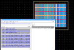
Hi guys I have an error that I can't understand why is happening:

It is the first one. This kind of error has to do with the contacts to the NWELL. I had this error before, but not for this kind of layout (mosfet that will serve as power devices).
As you can see I have the contacts to the well but he still gives the error. The description on the right I never saw before.
Does anyone knows why this is happening?
Last edited: