Continue to Site

Welcome to EDAboard.com

Welcome to our site! EDAboard.com is an international Electronics Discussion Forum focused on EDA software, circuits, schematics, books, theory, papers, asic, pld, 8051, DSP, Network, RF, Analog Design, PCB, Service Manuals... and a whole lot more! To participate you need to register. Registration is free. Click here to register now.

Return Path Capacitors

Status
Not open for further replies.

nickagian

Member level 4
Joined
Mar 19, 2009
Messages
71
Helped
2
Reputation
4
Reaction score
2
Trophy points
1,288
Location
Zurich, Switzerland
Activity points
2,001
Hi everyone!

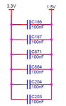
In the schematics of a reference design of an Ethernet Switch with 10G Interfaces, I have seen that the designer has used several capacitors that he called "Return Path Capacitors". These are 100nF and placed between the power supplies (see attachment). Some also placed towards ground.

Does anybody know what's the purpose of these capacitors? If yes, where should they be placed physically on the PCB? How many to use?

Thanks in advance!
Nikos
 

Attachments

  • return-path-caps.png
    return-path-caps.png
    16 KB · Views: 70

I would say that they are decoupling caps, the ones that connect to ground should be placed next to individual ICs as close to the supply pins as possible.
The purpose could be to filter high frequency's from getting into the IC's or as a fast respons voltage source, as the regulator or power source might not be able to supply enough current/voltage in the time frame that the IC needs it. I'm have little experience but such capacitors is often used to shorten the area or return path of loops where current is rapidly changing cous that creates a lot of EMI and in some cases ground currents.

But I might be wrong.

Thanks for your reply David. I already have some knowledge about placing such capacitors between power supplies and ground, but the thing is that here there are also caps between the different power supplies. I suppose their purpose is sth similar?
 

I have a ethernet switch bought that I can look at and see if there is any clue, I'll get back to you later today.
 

One common use for such things is when you have a high speed signal changing which plane it is referenced to.

Say you have a fast signal on layer 3 with a 3.3V plane on layer 4 and it is being moved to layer 6 with a 1.8V plane on layer 7, then you hight place a small cap between the planes right next to the signal vias so as to minimise the loop area for the return current flowing in the plane.

You really need a EM field solver to optimise this sort of thing, and it is one of the cases where the layout and schematic people really need to be one and the same.

Regards, Dan.
 
You've stumbled onto a reference to the black art of high speed design. In the high speed design world, high speed signals create high speed currents which require a high speed return path. Normal DC paths are too slow, but capacitors pass "AC", or quick changes of current very well. Thus caps are seen as providing a return path where other paths are seen as insufficient.

The idea of putting caps between different rails comes from the notion that a high speed line return current travels on the nearest plane that the high speed signal is "referenced" too (referenced meaning that it's the nearest plane, and the plane used for the purpose of impiedence calculations), regardless of the electrical signal that's on that plane.

If that nearby "reference' plane is split into multiple electrical signals then the idea is to have caps between those signals to provide a high speed path for the return current.

So if you see caps between rails study the layout and you'll surely see high speed lines crossing over gaps between those rails (or taking a via to another layer that's referenced to another signal). Generally this is just frowned upon however and you try to avoid having high speed lines change references at all (or if you must, at least make the change between ground and power - a pair that will already have decoupling caps). Putting caps between rails is just a great way to transmit noise from one rail to another.

All of this is rule of thumb stuff with varying levels of direct correlation to actual real world phenomena. But what works works.
 
THere is no obvious reason or relationship between this decoupling between 3.3 & 1.5V and Ethernet design, since there are no transient loads between these voltages. Decoupling to ground is all that is required unless there is something other than ethernet with a direct load or poor sensitivity to differential noise on these two rails.

Conclusion: There is no evidence of a forward path given, hence Return Path is not obvious.
 

I said I would get back a few days ago but time flew by, anyway since I said I would I just want to say that I looked over the Ethernet switch I have and it has no such capacitors.
It seems to indicate the validity of the claim made by SunnySkyGuy, the only decoupling caps that is on the board is between 3.3V and ground.
 

asdf44 hit the nail in the head. High speed electronics is as much black art as it is science.

One cannot "copy and paste" things. One must understand exactly what is being done and why is being done. And the reasons "why" many times are not obvious.

I've seen designs which will only work with a specific component vendor.....No substitutions allowed, even though in paper, both the specs appear to be identical.
 

Well, I should say the answers of asdf44 and Dan helped a lot in understanding the situation. And it is of course obvious that there is no relationship with the Ethernet design, that's true. Now I think I can apply a similar concept to my design as well.

There is sth I would like to clarify first. Let's assume we have the following PCB stack-up:

1 -> Signals and Ground
2 -> Ground
3 -> Signals
4 -> Power supply planes
(some bigger distance than between the other layers)
5 -> Power supply planes
6 -> Signals
7 -> Ground
8 -> Signals and Ground

So for signals on layers 1 and 8, the reference layer for return currents are layers 2 and 7, this is clear to me.

But what about signals on layers 3 and 6? Is it 4 and 5 or again 2 and 7?

The specific design I am talking about in this thread is implying that the responsible engineer has assumed the return currents are flowing over 4 and 5.

What do you think?

Nikos
 

Status
Not open for further replies.

Similar threads

Part and Inventory Search

Welcome to EDABoard.com

Sponsor

Back
Top