Continue to Site

Welcome to EDAboard.com

Welcome to our site! EDAboard.com is an international Electronics Discussion Forum focused on EDA software, circuits, schematics, books, theory, papers, asic, pld, 8051, DSP, Network, RF, Analog Design, PCB, Service Manuals... and a whole lot more! To participate you need to register. Registration is free. Click here to register now.

Altera Quad-Serial Configuration (EPCQ) Device

Status
Not open for further replies.

shaiko

Advanced Member level 5
Joined
Aug 20, 2011
Messages
2,644
Helped
303
Reputation
608
Reaction score
297
Trophy points
1,363
Activity points
18,302
Hello,

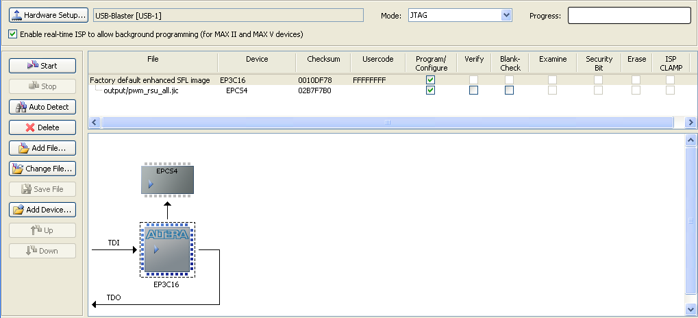
I'm working on a newly manufactured board that has an EPCQ Altera FLASH connected to a Cyclone IV FPGA in AS mode.
https://www.altera.com/literature/hb/cfg/cfg_cf52012.pdf

For some reason, I can't see the EPCQ memory in the JTAG scan chain - only the FGPA shows up.
As far as I understand, information in the above link suggests that I should instantiate a special core in the FPGA in order for it to communicate with FLASH in JTAG mode...am I right?
 

You can't directly communicate with the flash. You'll "attach" the flash device to the FPGA in the programmer window. If you choose a programmer operation for the flash, the default Altera flash loader will be automatically selected to be downloaded to the FPGA. A *.jic file has to be used for programming.

 
  • Like
Reactions: shaiko

    shaiko

    Points: 2
    Helpful Answer Positive Rating
You can't directly communicate with the flash
Is it because it's an EPCQ flash?

I remember using a POF file for FLASH programming...
What is the difference between JIC and POF ?
 

Is it because it's an EPCQ flash?
Not at all. The serial flash loader is working the same for single bit and quad bit serial flash. Both are SPI devices and don't "speak" JTAG.

*.jic is a special file format required by the Altera programmer tool when working in cooperation with the serial flash loader IP in FPGA. It's almost identical to the *.pof content but has a different header. It can't be generated during FPGA compilation directly but uses a separate "Convert Programming Files" tool. If you are using it regularly in a project, you can script the *.jic generation as post-flow.

I really suggest to review the Altera documentation about the matter.
 
  • Like
Reactions: shaiko

    shaiko

    Points: 2
    Helpful Answer Positive Rating
*.jic is a special file format required by the Altera programmer tool when working in cooperation with the serial flash loader IP in FPGA

When is it necessary to work with the flash loader IP ?
When can it be avoided ?
 

The SFL is necessary to access the flash by the programmer. Using the factory default image is one option, the other is to include a SFL instance in your application image. It consumes about 250 LEs with Cyclone II - IV.

Alternatively the flash can be programmed by the ALT_ASMI_PARRALEL IP from the application itself.
 
  • Like
Reactions: shaiko

    shaiko

    Points: 2
    Helpful Answer Positive Rating
When should I use POF ?
When should I use JIC ?
 

You should use what your hardware requires. POF for dedicated AS programming header, JIC for indirect JTAG programming (single programming header scheme).
 
  • Like
Reactions: shaiko

    shaiko

    Points: 2
    Helpful Answer Positive Rating
Understood.
According to the PCB's schematic the memory is connected serially to the FPGA as if it was a JTAG compatible device so it seems like JIC is what I need...

Anyways, the programmer shows an error message When I try to load the JIC file.

Can't recognize silicon ID for device 1
 

Sounds like incorrect EPCS wiring or wrong MSEL coding.
 
  • Like
Reactions: shaiko

    shaiko

    Points: 2
    Helpful Answer Positive Rating
Seems like both.
The designer didn't connect one of the configuration pins - nCE was floating.
This required an under BGA (!) conductor patch.

Now, I suspect the MSEL setting is wrong.
 

That's bad news. Probably no way to fix the prototype board.
 

For now, we fixed the nCE problem...
A really tiny copper strip patch between the unconnected (0.8mm pitch) nCE ball and a neighboring ground ball (the nCE is required to be shorted to ground).

Before that, we couldn't even burn the FPGA itself.
Now, the FPGA works but the memory fails to program.

I'm suspecting the MSELs - will have to check that.
 

Status
Not open for further replies.

Part and Inventory Search

Welcome to EDABoard.com

Sponsor

Back
Top