Continue to Site

Welcome to EDAboard.com

Welcome to our site! EDAboard.com is an international Electronics Discussion Forum focused on EDA software, circuits, schematics, books, theory, papers, asic, pld, 8051, DSP, Network, RF, Analog Design, PCB, Service Manuals... and a whole lot more! To participate you need to register. Registration is free. Click here to register now.

Sram read operation using switches in pspice

Status
Not open for further replies.

rajrevanth61

Member level 3
Joined
Mar 6, 2014
Messages
65
Helped
0
Reputation
0
Reaction score
0
Trophy points
6
Activity points
429
Hi,
Here is my code for SRAM for ead operation implemented using switches, can anyone help me where went wrong in the code, I am gettig both BL and BLB as high when i am trying to read a value of 1, which is stored in Q.

Please help

Code:
*source
vdd vdd 0 dc 2
 
CBL BL 0 1pf 
CBLB BLB 0 1pf 

*initial conditions stored for read operation
.ic v(Q)=1
.ic v(QR)=0


.ic v(bl)=1
.ic v(blb)=1 

*access control
vwl wl 0 pulse(0 2 4m 100u 100u 5m 6m)

*transistors used for latching
sw7 QR 0 Q  0 smod2

sw8 QR vdd Q vdd smod1

sw9 Q 0 QR  0 smod2

sw10 Q vdd QR vdd smod1


*transistors used for data access
sw11 bl Q wl  0 smod2
sw12 blb  QR wl 0 smod2

.tran 10m 100m uic 
.probe
.MODEL Smod1 VSWITCH(Ron=1000 Roff=1 Von=1V Voff=0.5V)
.MODEL Smod2 VSWITCH(Ron=1 Roff=1000 Von=1V Voff=0.5V)
 .end
 
Last edited by a moderator:
Reconsider the switch parameters. My PMOS transistor model would have a negative threshold voltage, just for clarity

Flipping Ron and Roff doesn't seem to serve a reasonable purpose, except confusing yourself. It's all about specifying suitable Von and Voff numbers and connecting the switches correctly.
 
Hello i tried the way you said, but Iam not getting the exact output still. Here is my code for inverter, can you please change the way you told me, so that it will be more easy for me to understand.

Please help me as i am very much need of this.

Code:
*inverternems*
vdd vdd 0 dc 1
vin 1 0 dc 1 
sw1 2 vdd   1 vdd Smod1
sw2 2   0   1 0 Smod2

.MODEL Smod1 VSWITCH(Ron=1000 Roff=1 Von=1V Voff=0.5V)
.MODEL Smod2 VSWITCH(Ron=1 Roff=1000 Von=1V Voff=0.5V)
.tran 1n 20u uic
.probe
.end
 
Last edited by a moderator:

Seems straightforward
Code:
.MODEL Smod1 VSWITCH(Ron=1 Roff=1000 Von=-1V Voff=-0.5V)
.MODEL Smod2 VSWITCH(Ron=1 Roff=1000 Von=1V Voff=0.5V)
 

But when i do the same for sram read operation, the output is same as the previous .
 

The inverter example simulates correctly with the suggested switch models.

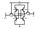
There are probably other problems with your "SRAM" simulation. I must confess that I don't understand the circuit. Perhaps you should sketch a schematic and explain what you expect.
 

Sram.PNG

This is the figure i have used for writing the netlist. I have initialized the conditions required for the read operation . i.e., I want to read a value of 1 so i have initialized Q as 1 and QR as 0. and for the read operation to take place both the bitlines have been initialized to 1.

with the suggested switch models, inverter is working fine, but there is some problem with the sram. Please help me.

Thank you
 

You shouldn't skip initial transient solution (uic option), otherwise SPICE jumps to a metastable operation point with ideal "transistors".

The "data access" switches are probably having no effect in this simulation setup. They are shorted by 1k resistors according to your switch model.
 

Can you please tinker the code accordingly as you said. this would be a great help to me.

Thanks a lot .
 

You shouldn't skip initial transient solution (uic option), otherwise SPICE jumps to a metastable operation point with ideal "transistors".

The "data access" switches are probably having no effect in this simulation setup. They are shorted by 1k resistors according to your switch model.

According to the code I am not skipping any initial condition. and what should I do in order to have a effect on the data access switches.

Please help me. I am stuck
 

[moved] Sram read operation using voltage controlled switches in pspice

Hi,
Here is my code for SRAM for read operation implemented using voltage controlled switches, can anyone help me where I went wrong in the code. both BL and BLB are loosing there voltage levels. when i am trying to read a value of 1, which is stored in Q.

I have also attached the schematic i have used for writing the netlist. I have initialized the conditions required for the read operation . i.e., I want to read a value of 1 so i have initialized Q as 1 and QR as 0. and for the read operation to take place both the bitlines have been initialized to 1.

Please help me
thank you


Sram.PNG

Code:
*sramnems*

*source
vdd vdd 0 dc 1
 

CBL BL 0 1pf 
CBLB BLB 0 1pf 


*initial conditions stored for read operation
.ic v(Q)=1
.ic v(QR)=0


.ic v(bl)=1
.ic v(blb)=1 


*access control
*vwl wl 0 pulse(0 2 4m 100u 100u 5m 5m)
vwl wl 0 pwl 0 0 200n 0 220n 1 400n 1 420n 0

*transistors used for latching
sw7 QR 0 Q 0 smod2

sw8 vdd QR Q 0 smod1

sw9 Q 0 QR 0 smod2

sw10 vdd Q QR 0  smod1


*transistors used for data access
sw12 bl Q wl 0 smod2
sw11 blb QR wl 0 smod2

.MODEL smod1 VSWITCH(Ron=1000 Roff=10000000 Von=-1V Voff=0V)
.MODEL smod2 VSWITCH(Ron=1000 Roff=10000000 Von=1V Voff=0V)


.tran 0.1n 1000n uic 

.probe

.end
Please help
 
Last edited by a moderator:

Status
Not open for further replies.

Part and Inventory Search

Welcome to EDABoard.com

Sponsor

Back
Top