Continue to Site

Welcome to EDAboard.com

Welcome to our site! EDAboard.com is an international Electronics Discussion Forum focused on EDA software, circuits, schematics, books, theory, papers, asic, pld, 8051, DSP, Network, RF, Analog Design, PCB, Service Manuals... and a whole lot more! To participate you need to register. Registration is free. Click here to register now.

autorouting with freerouting

Status
Not open for further replies.

nahidalam

Junior Member level 3
Joined
Apr 27, 2011
Messages
27
Helped
1
Reputation
2
Reaction score
1
Trophy points
1,283
Activity points
1,522
I am designing a medium complexity board using KiCAD. I am using freerouting tool to autoroute the design following the steps here **broken link removed**

Looks like autorouter keeps running forever with 7 connection still not done. I clicked on the violation tab and it says '5 clearance violation found'.

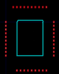
All the clearance violations shown in the tool are on different pins of the component footprints that I created (attached screenshot).

Can anyone please suggest here? Is it like the footprint I created itself violates the min clearance requirement? Or is there anything else?
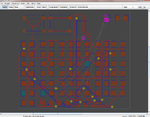
Untitled.png
 

I am an Eagle user, not a KiCAD user. Assuming some similarities, your assumption that the component you created is the problem seems correct. If you are certain the component cannot be made without violating the minimum clearance, then your option is to decrease the minimum clearance. That option might make getting a board manufactured a problem.

Some clearance problems can be ignored by the manufacturer. I had one recently that involved a via in a pad. The manufacturer said basically, "We agree it's needed, and we do it all the time. Don't worry." On the other hand, if it is a routing issue, that is another matter.

What component is it? What is your minimum clearance setting? Can you post a larger view of the component's footprint?

John
 

The min clearance setting in KiCAD is 0.254mm. Freerouting tool just uses that.

One of the component is TI CC2531 (https://www.ti.com/lit/ds/symlink/cc2531.pdf). The datasheet says it is VQFN-40 and yes, there is no QFN-40 footprint in KiCAD so I had to make one (attached).
May be I am not getting what 0,50/0,30 mean?

The other component is an Apple component. I replaced my footprint with KiCAD's SSOP-8 but still getting the clearance violation.

cc2531-PVQFN-40.png
 

I would start again at page 1 of the PCB design manual.
Your footprint is wrong, being able to create footprints is critical to using CAD, if you cant grasp that basic task then you are not going to be able to lay out PCBs (you have no thermal pad for a start).
You need to learn about spacing's and copper geometry sizes, again this is basic knowledge.
I don't know what the circuit is but the layout could be optimised, there are no obvious power tracks, there is no de-coupling! The main IC doesn't even have a pad for its GND connection. If you are going to use the rf function of this chip there is no way that layout is going to work.
My advice is look around this forum for threads on starting PCB design, read them. Read the software help notes etc that you are using and learn some basic electronics.
 
May be I am not getting what 0,50/0,30 mean?

My interpretation is 0.5 mm long and 0.3 mm wide based on the way the dimension lines are drawn. Near the end of the document, the recommended non-solder mask pad is shown as 0.28 mm wide. In either case, with a center to center spacing of 0.5 mm, the space between pad edges will be less than your minimum clearance of 0.254 mm (i.e., 0.20 mm and 0.22 mm, respectively).

EAGLE has that particular package in the TI library:

Capture.PNG

If you cannot import it, you may want to use it as a model to copy.

The board house I use does 6 mil spacing (0.15 mm) routinely. Clearly, you need to change that clearance setting in your program. This advice is only to address the clearance issue. The other issues mentioned above, including placement, also should be addressed.

John
 
Status
Not open for further replies.

Part and Inventory Search

Welcome to EDABoard.com

Sponsor

Back
Top