Continue to Site

Welcome to EDAboard.com

Welcome to our site! EDAboard.com is an international Electronics Discussion Forum focused on EDA software, circuits, schematics, books, theory, papers, asic, pld, 8051, DSP, Network, RF, Analog Design, PCB, Service Manuals... and a whole lot more! To participate you need to register. Registration is free. Click here to register now.

EAGLE schematic capture and board layout problems

Status
Not open for further replies.

TokTok12

Junior Member level 2
Joined
May 6, 2014
Messages
20
Helped
0
Reputation
0
Reaction score
0
Trophy points
1
Activity points
281
Hi all,

I’ve read quite a lot on different bits of advice on completing the schematic properly before embarking on any routing.

With regards to the routing I’ve read up on main aspects such as the selection of the routing grid in relation to the trace width, avoiding dimension errors and avoiding clearance errors.

Regarding my schematic I’ve got two components with each having a pin that I do not need to connect to anything at all. I’ve followed different pieces of advice and realized there is no “not connected” library in Eagle hence I created mine as per the following link. I then connect this custom symbol to my IC pin but no connection takes place and when I run my ERC check I come across the following errors in relation to both pins:

“No SUPPLY for POWER pin U1 TAB”.
“Unconnected INPUT pin IC1 ADJ”.

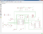
Here is my schematic: BGE ZIGBEE RELAY BOARD - 5 - HARDWARE  - 2ND SCHEMATIC BEFORE MANUAL AND AUTO ROUTING.png

In addition to the above problem, can anyone see any other issues with my schematic? Apart from the values of specific components which I intentionally deleted can anyone see any problem on my schematic that I might have not anticipated? Any help is appreciated.

Now moving on to the board routing (which BTW I undertook before realizing the above mentioned problem), I’ve come learn a lot in the recent days about the following things to watch out for when laying out components and subsequently undertaking the routing:

Selection of the routing grid (in relation to the trace width): I have a routing grid of10 mil and in the DRC sizes setting I have a minimum trace width of 10mil.
Selection of the trace width whilst watching out for current carrying traces.
Avoiding dimension errors.
Avoiding clearance errors.

The link below illustrates the placement of my components before I undertake manual routing and after but if need be auto routing. Just to mention in the image below I have already used the ratsnest tool.

BGE ZIGBEE RELAY BOARD - 5 - HARDWARE  - 2ND ATTEMPT - BOARD LAYOUT BEFORE MANUAL AND AUTO ROUTI.png

Can anyone please identify anything at all that would cause me a problem in any way?

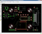
After the above I attempted manual routing and then auto-routing. As per my schematic above, I manually routed few but specific tracks those being power track to the +5v LDO voltage regulator and connections between the PIC18F2580 and each LED.

Below is my manually and then auto-routed board layout.

BGE ZIGBEE RELAY BOARD - 5 - HARDWARE  - Result of 1st auto-routing attempt.png

Could anyone kindly point out any issues I might face with regards to DRC and ERC plus any general advice?

Again any help is appreciated as it would save me time and effort solving errors.

Thanks,
TokTok.
 

Attachments

  • BGE ZIGBEE RELAY BOARD - 5 - HARDWARE  - SCHEMATIC BEFORE MANUAL AND AUTO ROUTING.png
    BGE ZIGBEE RELAY BOARD - 5 - HARDWARE - SCHEMATIC BEFORE MANUAL AND AUTO ROUTING.png
    89.2 KB · Views: 64
  • BGE ZIGBEE RELAY BOARD - 5 - HARDWARE  - BOARD LAYOUT BEFORE MANUAL AND AUTO ROUTING.png
    BGE ZIGBEE RELAY BOARD - 5 - HARDWARE - BOARD LAYOUT BEFORE MANUAL AND AUTO ROUTING.png
    143.2 KB · Views: 68

What did DRC and ERC show when you ran them? I suggest getting ERC done before routing.

1) I don't understand why you are concerned about setting the grid in "relation" to trace width. Where did you get that advice? What rule are your following?

2) It is much easier to find errors, such as unconnected pins and pads, if you attach the .brd and .sch files. Just put the two files in a folder and zip it for attachment to your post.

3) I don't understand why you needed a new symbol for a "not connected" pin. That happens quite often, e.g., when dealing with microprocessors and logic devices, and has never created a problem for me. When you say you created a new symbol, did you mean a new device (or device variant). A new symbol alone won't help.

Regards,

John

Hi John,

Thanks for the reply. Here is what the ERC gave me: BGE ZIGBEE RELAY BOARD - 5 - HARDWARE  - ERC ERRORS.png

I got the grid size in "relation" to trace width advice from this link:grid size in "relation" to trace width link

I've zipped and attached my .sch and .brd file. See: View attachment EASYDAQXBEE.rar

Regarding the creating of an NC symbol I should have said I attempted creating an NC device (with no package) which when I added into my schematic and attempted connecting to my NC pin of my component it didnt work.

On the flipside having read up more on NC pin it seems as long as a component does not need to be connected it can be left as it is. This is what I'm going to do with the two pins that the ERC as per the image above keeps identifying as error. I'm going to go ahead and approve the errors.

Thanks,
TokTok.
 

Re: Grid and traces

That link mentions grid five times. In each case, it is with respect to autorouting and pads/pins. You do need to have a grid spacing that will allow traces to attach to pads and pins. Prior to the more recent versions of Eagle, that was potentially a more serious problem. More recent versions snap to the center of pads. I have not had the need to test whether too large a grid affects that.

RE:ERC

I cannot find IC2 in your schematic. Is it U$2? You have Vcc connected to Vdd. Eagle gets sensitive about that.

The adjust of pin of IC1 needs to be connected. What is IC1? You only have two pins connected. Both are labeled GND.

All I have is Win7 on my PC. It doesn't open .rar, only .zip.

John

- - - Updated - - -

Update:

I just tested the assumption that snapping to the center of a pad was independent of the grid. I used an SMD device with a small pad spacing and a grid of 0.2 inch (alternative = 0.1 inch). Routing snapped to the center of each pad; although, the traces themselves followed the grid, as expected. Here's a snippet. Unfortunately, the grid doesn't show well. As implied previously, a situation of too large a grid for the devices being used seems unlikely to be encountered in practice. One might encounter something similar when using devices with metric packages on Imperial-dimension boards. That is where the snap to enhancement has be quite helpful.

Capture.PNG

John
 
Last edited:

Re: Grid and traces

That link mentions grid five times. In each case, it is with respect to autorouting and pads/pins. You do need to have a grid spacing that will allow traces to attach to pads and pins. Prior to the more recent versions of Eagle, that was potentially a more serious problem. More recent versions snap to the center of pads. I have not had the need to test whether too large a grid affects that.

RE:ERC

I cannot find IC2 in your schematic. Is it U$2? You have Vcc connected to Vdd. Eagle gets sensitive about that.

The adjust of pin of IC1 needs to be connected. What is IC1? You only have two pins connected. Both are labeled GND.

All I have is Win7 on my PC. It doesn't open .rar, only .zip.

John

- - - Updated - - -

Update:

I just tested the assumption that snapping to the center of a pad was independent of the grid. I used an SMD device with a small pad spacing and a grid of 0.2 inch (alternative = 0.1 inch). Routing snapped to the center of each pad; although, the traces themselves followed the grid, as expected. Here's a snippet. Unfortunately, the grid doesn't show well. As implied previously, a situation of too large a grid for the devices being used seems unlikely to be encountered in practice. One might encounter something similar when using devices with metric packages on Imperial-dimension boards. That is where the snap to enhancement has be quite helpful.

View attachment 105080

John

Hi John,

Thanks for the reply.

Re: Grid and traces

Where you mention "You do need to have a grid spacing that will allow traces to attach to pads and pins.", do you think that's the case with my board layout as seen here: BGE ZIGBEE RELAY BOARD - 5 - HARDWARE  - Result of 1st auto-routing attempt.png

I've noticed when manually routing two of the tracks as per the above mentioned layout what you mention with regards to the snapping of a track to the centre of the component pad. Thanks for highlighting that bit.

Re: ERC:

As per the UPDATED schematic diagram below IC2 is the MCP1703 3.3v LDO voltage regulator.

My UPDATED schematic can be seen here:BGE ZIGBEE RELAY BOARD - 5 - HARDWARE  - SCHEMATIC BEFORE MANUAL AND AUTO ROUTING.png

Its datasheet is can be seen here: **broken link removed**

As per the datasheet its Vin pin should be connected to Vdd hence I don't get why EAGLE isn't happy with this. Also as per the datasheet the tab pin is not connected.

Just for your information U$2 is a Telegesis ETRX357HR Zigbee module.

As per the UPDATED schematic above IC4 is the LM335 precision temperature sensor.

See the following link for the datasheet.
LM335 precision temperature sensor

Also the LM335 precision temperature sensor has its ADJ pin which clearly as per datasheet and more reading doesn't need a connection.

To move on I have approved these two errors as I believe there is no error with regards to the pins on both ICs remaining not connected.

The reason why two of the pins are labelled GND is due to the custom library I used which labels the pin connected to the PIC18F2580 as ground as opposed to Vout. On the schematic the pin connected to the PIC18F2580 should read Vout not GND but this does not affect the package and the board layout. The custom library was built from a component/device with the exact footprint i.e. the LM35 precision temperature sensor.

As for my .sch and .brd files I've attached them as seen below as .zip.

View attachment EASYDAQ-XBEE v4sch.zip

Thanks,
TokTok.
 

Where you mention "You do need to have a grid spacing that will allow traces to attach to pads and pins.", do you think that's the case with my board layout as seen here:...

I guess I wasn't clear, as I was not sure when I wrote that how the "snap to" would work with a very large grid. In early versions of Eagle, traces did not automatically go to the center of pads. That is no longer the case. As I demonstrated, the grid can be considerably larger than the pad spacing, and the trace will find the pad. I don't think doing so is a good idea. With anything at all complex, having a large grid size and small pad spacing will look quite odd and waste a lot of space. I don't know whether it would affect autorouting and haven't checked. I rarely use autorouting, except early on in a board design to get a feel for problem areas.

The reason why two of the pins are labelled GND is due to the custom library I used which labels the pin connected to the PIC18F2580 as ground as opposed to Vout. On the schematic the pin connected to the PIC18F2580 should read Vout not GND but this does not affect the package and the board layout. The custom library was built from a component/device with the exact footprint i.e. the LM35 precision temperature sensor.
I see what you have done there. Despite the apparent label of GND, it is really its own net ,(N$94). It will likely work this time, but I would not recommend doing that routinely. It would be confusing to anyone who didn't have access to the sch file. It is easy to just open the device in Library Editor, name the pins properly, fix connections (if necessary), and save as a variant or new device.

John
 

Hi all,

After taking into consideration the above replies to my post I've developed my board to the silkscreen stage.

A screenshot of my schematic and board layout progress can seen on the following attachment:

**broken link removed**

Please refer to my earlier post for my schematic.

Now when I run my DRC all is well apart from the numerous stop mask error I'm encountering. Having done some research regarding the error it seems generally the cause is the TPlace or TNames layers overlaps the solder mask apertures - I got that from here.

How do I solve this issue?

Thanks,
TokTok.
 

Status
Not open for further replies.

Part and Inventory Search

Welcome to EDABoard.com

Sponsor

Back
Top