Continue to Site

Welcome to EDAboard.com

Welcome to our site! EDAboard.com is an international Electronics Discussion Forum focused on EDA software, circuits, schematics, books, theory, papers, asic, pld, 8051, DSP, Network, RF, Analog Design, PCB, Service Manuals... and a whole lot more! To participate you need to register. Registration is free. Click here to register now.

Cannot understand the acknowledgement signal in I2c Bus-ADS1015 TI ADC chip

Status
Not open for further replies.

kunal5959

Junior Member level 3
Joined
Jul 26, 2011
Messages
31
Helped
0
Reputation
0
Reaction score
0
Trophy points
1,286
Activity points
1,644
Screenshot_1.png


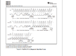
I have to access the ADC chip ADS1015 by sending data throughI2c bus. In the data sheet Yellow box highlights Read/write bit, Green is ACKnowledgement bit and the Red box is something which i do not understand, what it means. After that the second byte of data is sent to ADS1015.
Do i have to worry about generating that peak( inside red box). Can anyone suggest me what that peak means, or is it just a way showing end of 1st frame of data and beginning of second frame of data.
 

Attachments

  • Screenshot_1.png
    Screenshot_1.png
    103.8 KB · Views: 112

In the green box the master sends a '1' (really open collector with pull-up). The ack bit is generated by the slave, which during one bit (the green box) activates it's driver on the SDA line to send a '0'.
When the slave stops driving the SDA to '0' it can take some time before the master starts driving a '0' for the next byte. SDA will be pulled towards '1' when nothing is driving it to '0'. This is the reason for the possible "glitch" in the red box.
 
Thanks a lot for the reply. That really helped in understanding the SDA glitch better.
 

Status
Not open for further replies.

Part and Inventory Search

Welcome to EDABoard.com

Sponsor

Back
Top