Continue to Site

Welcome to EDAboard.com

Welcome to our site! EDAboard.com is an international Electronics Discussion Forum focused on EDA software, circuits, schematics, books, theory, papers, asic, pld, 8051, DSP, Network, RF, Analog Design, PCB, Service Manuals... and a whole lot more! To participate you need to register. Registration is free. Click here to register now.

Help Simulating Dickson Charge Pump

Status
Not open for further replies.

Insidious

Newbie level 4
Joined
Mar 4, 2014
Messages
6
Helped
0
Reputation
0
Reaction score
0
Trophy points
1
Activity points
58
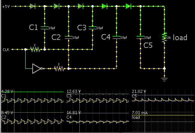
Hello, I am trying to build and simulate a Dickson Charge Pump in Cadence Virtuoso for class. I need it to bump 1v to 3v. Should be simple enough but the circuit I built is not wokring correctly.

Below are my schematics and output wave forms.

CPtest.png
DCP.png
Inverter.png
test.png

I used the design from wikipedia; I've tried various transistor widths and lengths and also different capcitor values, but I never get more than 1V at the output. My inverter is sized 12/3um (W/L). The clock has a 1ns period and a 500ps pulse width. Not sure what else to try, any pointers?

I don't necessarily need a Disckson charge pump, but it seemed the simplest one to try. Also I cannot use diodes (NCSU libraries don't have diode models), so i must stick to NMOS for the switches.

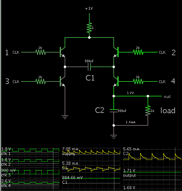
I've also tried this design, even though it is more complicated (from a class slide):
Screenshot from 2014-05-04 04:28:06.png
CP.png

But I just get low voltage at the output.

Any help is appreciated. Thanks in advance.
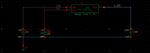
 

Attachments

  • CPtest.png
    CPtest.png
    5.7 KB · Views: 273
  • test.png
    test.png
    174.9 KB · Views: 276

Can you decrease Cout to (500/3)n
 

Without knowing much about Dickson, or what a normal NMOS W/L ratio should be, my thoughts turned to the following -- are you constrained to using a 1Ghz clock ? Wouldn't something slower be more appropriate and allow your caps to actually charge/ discharge through real-world impedances ?
 
At 1GHz you're probably sloching current in and out of the
caps without much "pumping".

At 1V gate drive, your FETs may be a big loss term, you
only can pump forward Vdd-Vt or so.

500nF capacitors are pretty damn big for a little integrated
FET to drive, a DC solution of VOUT=VDD can be reached
but no further pumping is evident - but this might be a
timescale vs capacitor value problem.

Consider making your pump FETs synchronous rather than
making them act like passive diodes. You'll kill the forward
drop that way. But you'll need level shifting of some sort,
which may put you on the wrong side of some isolation
limit perhaps.
 
I'm running a simulation of the doubler.

The switching arrangement resembles an H-bridge.

Your capacitors are labelled 500 nF. To get them to show charge-pump behavior, I reduced the frequency to 50 kHz.


Bias voltages are shown. These demonstrate what levels are necessary to operate the transistors/mosfets. They are N-devices in the simulation.
This is not to say P-devices cannot be used, however.

The tripler will add a similar H-bridge stage.
 

Ok so from the hints you guys gave me, I raised the aplitude of the clock from 1V to 2.5V and tweaked the clock to T=500us/PW=250us (2kHz) and I started to see some results:

ChargePump50fF.pngChargePumpResults50fF-2.png
ChargePump50kOhm.pngChargePumpResults50kOhm-2.png

The first set of images are for a load with a 50fF capacitor; the second are for a load of a 50k Ohm resistor.

However, I must now simulate with a load of 1k Ohm, and now no matter what combination of capacitor of frequency, I cannot generate more than 0.75V. I've tried 1fF-1F (yes 1F), in power of 10 increaments (1, 10, 100, 1000), and frequency of 100Hz-1MHz:

CP1kOhmtest.pngtest2.png

The only way I could generate about 1.25V was using an initial voltage of 4V, so I'm guesing I've reached the limits of this configuration and now it is acting like a voltage downscaler.

Any suggestions?
 

The final capacitor will charge to the output voltage. The neighboring mosfet needs to be biased several volts higher than that.

In fact, it's a good idea to check whether each mosfet is turning on entirely, and off entirely.
 

The best I could do was just put 6 of them in parallel in order to get the 3V.

ChargePump1kOhmtest-2.pngChargePumpResults1kOhm-2.png

Not the best solution, but it came to turn it in or get no credit.

Thanks anyways, hopefully this helps someone out there as well. :cool:
 

Since you obtained some output, you demonstrated the concept.

I believe the problem is that the mosfets were barely turning on. They are meant to act as diodes. However they are biased only a volt or so at the time they turn on.

I made a simulation of one of your schematics which contains one invert-gate. I chose a 5V supply voltage, because the invert-gate puts out 5V.


I chose a light load (3k ohms) to maintain output voltage near maximum.
This is called a x5 multiplier (nominally). However it loses a few volts due to diode drops, and parasitic resistances.

So if this is what I get with a 5V supply, then you were doing well to get any increase with a 1V supply.
 

Status
Not open for further replies.

Part and Inventory Search

Welcome to EDABoard.com

Sponsor

Back
Top