Welcome to our site! EDAboard.com is an international Electronics Discussion Forum focused on EDA software, circuits, schematics, books, theory, papers, asic, pld, 8051, DSP, Network, RF, Analog Design, PCB, Service Manuals... and a whole lot more! To participate you need to register. Registration is free. Click here to register now.
Could you explain how to choose the worst cases for rising and falling?
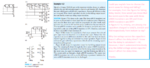
For example, from the figure for falling delay model, how would you know that the worst case is the case
with three nMOS transistors are ON and three pMOS transistors are OFF?
No, the worst case (w.c.) for falling delay is when initially three nMOS transistors are OFF and three pMOS transistors are ON (all inputs LOW, output is HIGH), and all inputs simultaneously go HIGH (output falls LOW), because in this case all caps (9C, 3C, 3C) must be discharged simultaneously.
The resistors in figure 4.7 (d) don't exist, as the corresponding transistors initially (and ideally) are OFF. Hence the voltage distribution would be inverse to the caps' values, i.e. Vdd*3/7 , Vdd*6/7 , and Vdd from bottom to top. In practice there are still leakage currents through the transistors also in their OFF state, so the voltage distribution will be somewhere between the above mentioned state and the Vdd/3, 2Vdd/3, Vdd distribution mentioned by you.
Why the voltage across the capacitors doesn't affect the delay time? I know that the delay is calculated t = RC.
However, I don't understand intuitively why the initial voltage across capacitor doesn't affect the delay time.
Actually, it does. In the w.c. falling delay consideration mentioned above, the longest fall time stems from the discharge of the transistor node closest to the output (9C). The discharge time of the two lower nMOS caps is by a factor of 3 lower and starts simultaneously with the discharge of the 9C node, so only marginally prolongs the total falling delay time.
So the a.m. w.c. falling delay time is only insignificantly longer than the case from initially having the two "lower" inputs already HIGH, and setting only the "highest" input - which leads to the nMOS closest to the output - to HIGH.
This site uses cookies to help personalise content, tailor your experience and to keep you logged in if you register.
By continuing to use this site, you are consenting to our use of cookies.