Continue to Site
Follow along with the video below to see how to install our site as a web app on your home screen.
Note: This feature may not be available in some browsers.
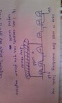
Standard CMOS processes tend to be P- substrate (epi
over P+ handle, when economics support that cost, or
plain bulk P- all the way down for the cheapest wafer).
An N-well is needed for standard voltage PMOS. Its Xj
will be just what is needed to not punch through, the
highest PMOS S/D voltage to the grounded substrate.
Its doping will be low enough that no zener / avalanche
action will occur at max VDD-VSS.
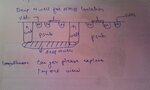
For a P+ region that needs higher voltage, or a NWell that
likewise has to exceed "normal", the well doping will be
brought down and the Xj made deeper. This will let you do
high voltage PMOS, may serve as the drain region for an
extended-drain or LDMOS N-channel, or may house yet
another P- region for floating NMOS (twin well or triple
well).
Every well has a parasitic diode. The deep NWell diode
should have a higher breakdown, a more rounded junction
(also helping BV) due to more side diffusion, possibly lower
leakage (depending on whether impact ionization, or
depletion volume generation current is more significant)
than a standard NWell.