Continue to Site

Welcome to EDAboard.com

Welcome to our site! EDAboard.com is an international Electronics Discussion Forum focused on EDA software, circuits, schematics, books, theory, papers, asic, pld, 8051, DSP, Network, RF, Analog Design, PCB, Service Manuals... and a whole lot more! To participate you need to register. Registration is free. Click here to register now.

Difference between solder mask and paste mask in gerber files

Status
Not open for further replies.

Techetok

Newbie level 4
Joined
Jan 12, 2014
Messages
6
Helped
0
Reputation
0
Reaction score
0
Trophy points
1
Activity points
58
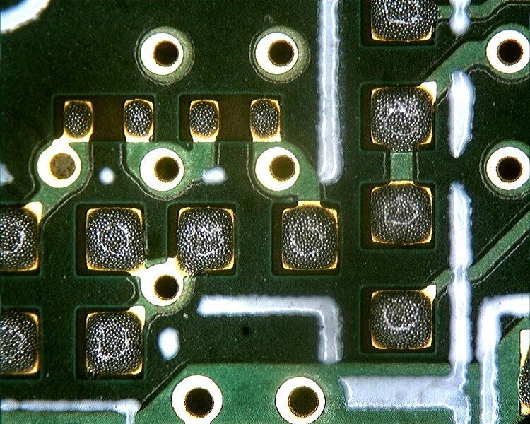
What's the difference between solder mask and paste mask layers in gerber files? I don't quite get it and there is no obvious place to read about it either.
p.s. I'm not quite sure where this topic belongs, so I put it here
 

Have a look at arbitrary PCB boards in your reach. I'm sure you'll find on most boards solder mask openings that aren't printed with solder paste, e.g. all through plated pins.

Secondly, solder mask and paste pads undergo different size modifications according to technology requirements.
 

So the paste mask should be smaller that the solder mask? In the image here
750px-Solder_Paste_Printed_on_a_PCB.jpg

is the silverish thing solder mask and the spot-patterned thing on top of it - paste mask? Did I get it right?
 

Absolutely right. You also notice that the vias have an opening in solder mask but no paste printed on it.

The photo is showing a bad design detail, some pads next to a via without separating solder mask bar. Solder might drain into the via, resulting in unreliable solder joints.
 

Status
Not open for further replies.

Part and Inventory Search

Welcome to EDABoard.com

Sponsor

Back
Top