Continue to Site

Welcome to EDAboard.com

Welcome to our site! EDAboard.com is an international Electronics Discussion Forum focused on EDA software, circuits, schematics, books, theory, papers, asic, pld, 8051, DSP, Network, RF, Analog Design, PCB, Service Manuals... and a whole lot more! To participate you need to register. Registration is free. Click here to register now.

Switched Capacitor Circuits Transient Simulation on Cadence

Status
Not open for further replies.

ashourism

Newbie level 6
Joined
May 17, 2012
Messages
12
Helped
0
Reputation
0
Reaction score
0
Trophy points
1,281
Location
Egypt
Activity points
1,381
Hi,

i am trying to simulate a basic ideal switched cap circuit to make a non inverting amplifier based on on analysis in Ch.12 of Razavi's : Design of Analog CMOS Integrated Circuits, ofc due to copyright i couldn't upload more than those two pictures but please if you have the book try to read the circuit description

Razavi's Circuit 1.png

Razavi's Circuit 2.png

What i understand is that when S1, S2 Closes Q(C1) = Vin*C1, then When S1,S2 Opens and S3 Closes it pushes V(C1) to zero given that feedback through C2 pushes the node between C1 and C2 to ground, and due to charge transfer and applying
Q(Total) = Vin* C1 = 0*C1 + Vout * C2 thus Vout = (C1/C2) * Vin

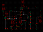
am using Cadence IC511, transient analysis however i am really unable to get any reasonable results my circuit is attached i am using ideal switches from Analog Lib

Open Voltage =0.999
Close Voltage = 1.00001
ROpen = 1TOhm
Rclose = 100uOhm

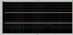
The Switch Transfer Characterstics was simulated lonely to check it first using this circuit, using a DC analysis with a sweep on Vcontrol from -3v to +3v

Switch Test Circuit:
Ideal Switch Test.png

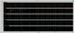
Switch Test Circuit Output
Switch Output.png


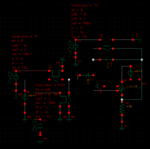
Non-Inverting Switched Capacitor Circuit, Clks are displayed on the circuit below
Circuit.png

note : I also used an Ideal high gain OTA Model for the OpAmp using a VCCS from AnalogLib and an Rout of 1MOhm
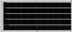
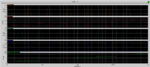
Simulated Output of Non-Inverting Switched Capacitor Circuit :
Wrong Output.png

I hope some one can help me with this

Thanks
 

I believe you are connecting the switch that is driven by phi2 wrong. Check it to make sure.

Other than that, I can give you some friendly advice that might make your life easier:

1- If you are not going to model and opamp, just use vcvs, simpler, easier and more reliable.
2- You are giving way long non overlap time between signals. It might not be problem for ideal case, but it definitely is for non-ideal.
3- Draw neat schematics, this way you will be less prone to make errors.
4- This won't work in single supply cmos realization, simply because the virtual ground is 0. You should use a reference voltage if necessary.

Try it and let me know the results.

Edit: By wrong, I mean the clock signal is not right.
 
Last edited:
I believe you are connecting the switch that is driven by phi2 wrong. Check it to make sure.

Other than that, I can give you some friendly advice that might make your life easier:

1- If you are not going to model and opamp, just use vcvs, simpler, easier and more reliable.
2- You are giving way long non overlap time between signals. It might not be problem for ideal case, but it definitely is for non-ideal.
3- Draw neat schematics, this way you will be less prone to make errors.
4- This won't work in single supply cmos realization, simply because the virtual ground is 0. You should use a reference voltage if necessary.

Try it and let me know the results.

Edit: By wrong, I mean the clock signal is not right.

First of all thanks for help, however I am not sure what can be wrong with this switch can you illustrate more? also I don't understand point four do you mean I shouldn't connect the switch to gnd and I should use a Vdc and set it to zero?

Thanks
 

In your switch simulations, you have connected the node with the instance notation (W0) upside. But for the switch I mentioned it is connected to the bottom. So when both phi1 and phi2 are zero, you are integrating the offset error of the amplifier. Can you check that and let me know if that is the problem?

If you try to establish a virtual ground at 0 DC level, your opamp will fail simply because the output range of your opamp can never include 0 unless you use two supply voltages.

I followed your suggestion and i got a significant change in output it follows however its not 2Vin its 1V during Phase2 and till phase1 comes again also there are some glitches that i can't interpret it

Edit: i forgot to set C1 to 2 pF for Vout = 2Vin. however what about the glitches any suggested interpretation?

Thanks
 

Attachments

  • Fixed Circuit 1.png
    Fixed Circuit 1.png
    21.1 KB · Views: 299
  • new output.png
    new output.png
    40.5 KB · Views: 265
Last edited:

So first of all, if you are serious in this vlsi thing, I have a few more suggestions. Exactly know what you are expecting. You should guess how each node will behave, simulator should give you the exact answer, it can't design it for you, it just verifies that your initial thought was correct.

Why am I telling you this, simply because this is the expected result. If you are asking why it reaches 0, the answer is because it is supposed to. In sampling phase, the opamp is connected in voltage buffer configuration, therefore forces the bottom plate of the cap to gnd, which is short circuited to the output. That's why you are getting zeroes every period.

In the other phase, the charge on a large cap is forced to be dumped on a small cap, creating a voltage amplification. So the output tries to reach this voltage as the feedback forces it to. But if the circuit was truly ideal, it should have reached those voltages instantly. However, instant transitions create discontinuities and can't be processed by most of the modern simulators. So you are forced to select on and off resistors for your switches while using cadence. This res+cap combination creates poles, even though your ideal opamp has no poles or zeroes, the poles generated by res+cap move around the frequency domain as you close the loop. This is a terribly high frequency since you have selected very low resistances and considerably small capacitances. So your loop settles extremely fast, but has a phase margin less than 90 degrees therefore it overshoots, creating the spikes you don't seem to like :D

There are much more simple and intuitive explanations for this phenomena but I had nothing to do, so I have written this one.

Edit: I'm not busy right now so let's continue, a more intuitive way to explain this is using the electromagnetic equations and device behaviour. As basics are concerned, the caps try to establish a constant voltage while inductances establish a constant current. So your cap follows an equation like C* dVc/dt, what do you think would happen if you were to change Vc very quickly. CHARGE MOSH PIT, that's what happens, so basically at the end of charging, you are forcing a voltage change in your transition time of the clock signal which starts mosh pit. What you can do is simple, you can increase the RC constant to regulate the flow of charge, which in turn reduces your maximum clock speed. Or you can allow glitches to occur at a much higher frequency than your interested region. The second one is more beneficial for signal processing, since you want your signals to be extremely linear in this case. The first one is, not always, but sometimes used to optimize the switch sizes and cap sizes for switch cap dc-dc converters, because in this type of converters every micron of switch you drive returns as loss which degrade the efficiency and as long as you transfer enough charge to the output you are fine.
 
Last edited:
Really i can't find words to thank you, i am now trying to use my basic knowledge of switched cap to simulate this precision multiply by 2 and subtraction (MDAC) circuit used in pipelined ADC

its based on the circuit shown here https://www.iadc.ca/Imran_Pipeline_ADC_tutorial_files/image003.gif

its explanation : https://www.iadc.ca/Pipeline_ADC_tutorial.htm#1.3

I made the circuit on Cadence and simulated it but the output seems to be right only for the first cycle then it starts to build up as if there is some positive feedback taking place, this doesn't happen when i put Vref = 1;

i also plotted a node which is the left plate of C4 which seems to be the cause of this build up when Vref = 0, -1

Thanks again
 

Attachments

  • Vref = -1.png
    Vref = -1.png
    19.8 KB · Views: 188
  • Verf = 1.png
    Verf = 1.png
    18.9 KB · Views: 154
  • Verf = 0.png
    Verf = 0.png
    19.1 KB · Views: 202
  • MDAC Circuit.png
    MDAC Circuit.png
    18 KB · Views: 208
Last edited:

Man, this is too much to debug. First, your schematics really look complicated, and second too many clock phases to follow. Work on it and see if you can come up with a neat problem definition. Otherwise, it is too long, I didn't even read :D

But here one quick thing that caught my attention, why did you connect one of the control voltage nodes of W11 to its switch side? This is kind of meaningless since they are already ideal, and you are not trying to model power consumption or switch linearity.
 
You know what W11 was the actual problem LOL :D

man you are like a miracle that happened over the last two days in my life

Thanks!
 

Status
Not open for further replies.

Part and Inventory Search

Welcome to EDABoard.com

Sponsor

Back
Top